- 您現在的位置:買賣IC網 > PDF目錄373944 > AD8349ARE-REEL7 (ANALOG DEVICES INC) 700 MHz to 2700 MHz Quadrature Modulator PDF資料下載
參數資料
| 型號: | AD8349ARE-REEL7 |
| 廠商: | ANALOG DEVICES INC |
| 元件分類: | 衰減器 |
| 英文描述: | 700 MHz to 2700 MHz Quadrature Modulator |
| 中文描述: | 700 MHz - 2700 MHz RF/MICROWAVE QPSK MODULATOR |
| 封裝: | MO-153ABT, TSSOP-16 |
| 文件頁數: | 6/28頁 |
| 文件大小: | 969K |
| 代理商: | AD8349ARE-REEL7 |
第1頁第2頁第3頁第4頁第5頁當前第6頁第7頁第8頁第9頁第10頁第11頁第12頁第13頁第14頁第15頁第16頁第17頁第18頁第19頁第20頁第21頁第22頁第23頁第24頁第25頁第26頁第27頁第28頁
AD8349
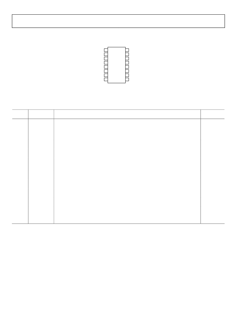
PIN CONFIGURATION AND FUNCTIONAL DESCRIPTIONS
Rev. 0 | Page 6 of 28
AD8349
TOP VIEW
(Not to Scale)
IBBP
1
IBBN
2
COM1
3
COM1
4
LOIN
5
QBBP
QBBN
COM3
COM3
VPS2
15
14
13
12
LOIP
6
VPS1
7
ENOP
8
VOUT
COM3
COM2
11
10
9
16
0
Figure 2
Table 3. Pin Function Descriptions
Pin No.
1, 2,
15, 16
Mnemonic
IBBP, IBBN,
QBBN, QBBP
Description
Differential In-Phase and Quadrature Baseband Inputs. These high impedance inputs must be
dc-biased to approximately 400 mV dc, and must be driven from a low impedance source.
Nominal characterized ac signal swing is 600 mV p-p on each pin (100 mV to 700 mV). This
results in a differential drive of 1.2 V p-p with a 400 mV dc bias. These inputs are not self-biased
and must be externally biased.
Common Pin for LO Phase Splitter and LO Buffers. COM1, COM2, and COM3 should all be
connected to a ground plane via a low impedance path.
Differential Local Oscillator Inputs. Internally dc-biased to approximately 1.8 V when V
S
= 5.0 V.
Pins must be ac-coupled. Single-ended drive is possible with degradation in performance.
Positive Supply Voltage (4.75 V to 5.25 V) for the LO Bias-Cell and Buffer. VPS1 and VPS2 should
be connected to the same supply. To ensure adequate external bypassing, connect 0.1 μF and
100 pF capacitors between VPS1 and ground.
Output Enable. This pin can be used to enable or disable the RF output. Connect to high logic
level for normal operation. Connect to low logic level to disable output.
Common Pin for the Output Amplifier. COM1, COM2, and COM3 should all be connected to a
ground plane via a low impedance path.
Common Pin for Input V-to-I Converters and Mixer Cores. COM1, COM2, and COM3 should all
be connected to a ground plane via a low impedance path.
Device Output. Single-ended, 50 internally biased RF output. Pin must be ac-coupled to the
load.
Positive Supply Voltage (4.75 V to 5.25 V) for the Baseband Input V-to-I Converters, Mixer Core,
Band Gap Reference, and Output Amplifer. VPS1 and VPS2 should be connected to the same
supply. To ensure adequate external bypassing, connect 0.1 μF and 100 pF capacitors between
VPS2 and ground.
Equivalent
Circuit
Circuit A
3, 4
COM1
5, 6
LOIN, LOIP
Circuit B
7
VPS1
8
ENOP
Circuit C
9
COM2
10, 13,
14
11
COM3
VOUT
Circuit D
12
VPS2
相關PDF資料 |
PDF描述 |
|---|---|
| AD8350 | Low Distortion 1.0 GHz Differential Amplifier |
| AD8350AR15 | Low Distortion 1.0 GHz Differential Amplifier |
| AD8350AR15-EVAL | Low Distortion 1.0 GHz Differential Amplifier |
| AD8350AR15-REEL | Low Distortion 1.0 GHz Differential Amplifier |
| AD8350AR15-REEL7 | Low Distortion 1.0 GHz Differential Amplifier |
相關代理商/技術參數 |
參數描述 |
|---|---|
| AD8349AREZ | 功能描述:IC QUADRATURE MOD 700MHZ 16TSSOP RoHS:是 類別:RF/IF 和 RFID >> RF 調制器 系列:- 產品培訓模塊:Lead (SnPb) Finish for COTS Obsolescence Mitigation Program 標準包裝:2,500 系列:- 功能:調制器 LO 頻率:700MHz ~ 2.3GHz RF 頻率:700MHz ~ 2.3GHz P1dB:1dBm 底噪:-148dBm/Hz 輸出功率:-1dBm 電流 - 電源:46mA 電源電壓:2.7 V ~ 3.6 V 測試頻率:1.75GHz 封裝/外殼:28-WFQFN 裸露焊盤 包裝:帶卷 (TR) |
| AD8349AREZ-RL7 | 功能描述:IC MOD QUAD 2.7GHZ 16TSSOP RoHS:是 類別:RF/IF 和 RFID >> RF 調制器 系列:- 產品培訓模塊:Lead (SnPb) Finish for COTS Obsolescence Mitigation Program 標準包裝:2,500 系列:- 功能:調制器 LO 頻率:700MHz ~ 2.3GHz RF 頻率:700MHz ~ 2.3GHz P1dB:1dBm 底噪:-148dBm/Hz 輸出功率:-1dBm 電流 - 電源:46mA 電源電壓:2.7 V ~ 3.6 V 測試頻率:1.75GHz 封裝/外殼:28-WFQFN 裸露焊盤 包裝:帶卷 (TR) |
| AD8349EVAL | 制造商:Analog Devices 功能描述:IC ((NS)) |
| AD8349-EVAL | 制造商:Analog Devices 功能描述:AD8349 EVALUATION BOARD - Bulk |
| AD8349-EVALZ | 制造商:Analog Devices 功能描述:AD8349 EVALUATION BOARD - Bulk |
發布緊急采購,3分鐘左右您將得到回復。