- 您現在的位置:買賣IC網 > PDF目錄373945 > AD835AR (ANALOG DEVICES INC) 250 MHz, Voltage Output 4-Quadrant Multiplier PDF資料下載
參數資料
| 型號: | AD835AR |
| 廠商: | ANALOG DEVICES INC |
| 元件分類: | 運動控制電子 |
| 英文描述: | 250 MHz, Voltage Output 4-Quadrant Multiplier |
| 中文描述: | ANALOG MULTIPLIER OR DIVIDER, 250 MHz BAND WIDTH, PDSO8 |
| 封裝: | PLASTIC, SOIC-8 |
| 文件頁數: | 7/8頁 |
| 文件大小: | 200K |
| 代理商: | AD835AR |
AD835
REV. A
–7–
APPLIC AT IONS
T he AD835 is both easy to use and versatile. T he capability for
adding another signal to the output at the Z input is frequently
valuable. T hree applications of this feature are presented here: a
wideband voltage controlled amplifier, an amplitude modulator
and a frequency doubler. Of course, the AD835 may also be
used as a square law detector (with its X - and Y-inputs con-
nected in parallel) in which mode it is useful at input frequen-
cies to well over 250 MHz, since that is the bandwidth
limitation only of the
output
amplifier
.
Multiplier Connections
Figure 18 shows the basic connections for multiplication. T he
inputs will often be single sided, in which case the X 2 and Y2
inputs will normally be grounded. Note that by assigning Pins 7
and 2 to these (inverting) inputs, respectively, an extra measure
of isolation between inputs and output is provided. T he X and
Y inputs may, of course, be reversed to achieve some desired
overall sign with inputs of a particular polarity, or they may be
driven fully differentially.
Power supply decoupling and careful board layout are always
important in applying wideband circuits. T he decoupling rec-
ommendations shown in Figure 18 should be followed closely.
In remaining figures in this data sheet, these power supply
decoupling components have been omitted for clarity, but
should be used wherever optimal performance with high speed
inputs is required. However, they may be omitted if the full high
frequency capabilities of AD835 are not being exploited.
A Wideband Voltage Controlled Amplifier
Figure 19 shows the AD835 configured to provide a gain of
nominally 0 to 12 dB. (In fact, the control range extends from
well under –12 dB to about +14 dB.) R1 and R2 set the gain to
be nominally
×
4. T he attendant bandwidth reduction that
comes with this increased gain can be partially offset by the ad-
dition of the peaking capacitor C1. Although this circuit shows
the use of dual supplies, the AD835 can operate from a single
9 V supply with slight revision.
Figure 19. Voltage Controlled 50 MHz Amplifier Using the
AD835
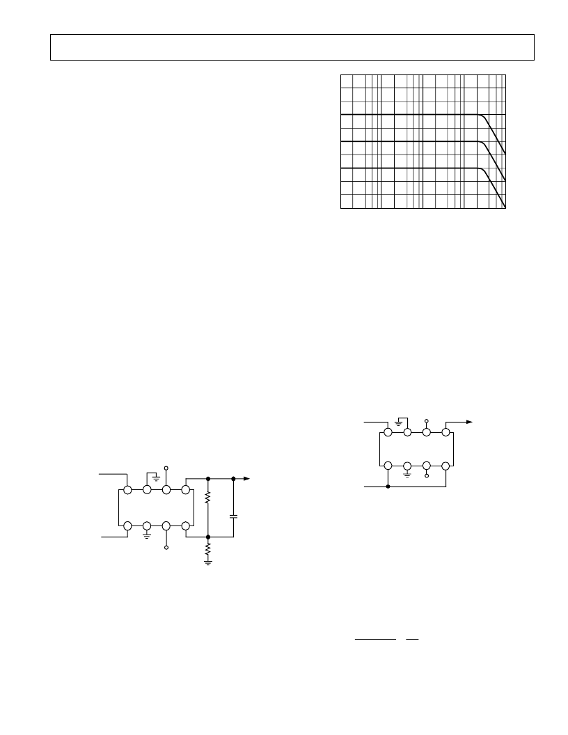
T he ac response of this amplifier for gains of 0 dB (V
=
0.25 V), 6 dB (V
= 0.5 V) and 12 dB (V
= 1 V) is shown in
Figure 20. In this application, the resistor values have been
slightly adjusted to reflect the nominal value of U = 1.05 V. T he
overall sign of the gain may be controlled by the sign of V
G
.
V
(SIGNAL)
R2
301
VOLTAGE
OUTPUT
X1
X2
AD835
VP
W
Z
4
VN
3
Y2
2
Y1
1
X1
+5V
–5V
R1
97.6
5
6
7
8
C1
33pF
V
(GAIN CONTROL)
Figure 20. AC Response of VCA
An Amplitude Modulator
Figure 21 shows a simple modulator. T he carrier is applied both
to the Y-input and the Z-input, while the modulating signal is
applied to the X -input. For zero modulation, there is no product
term, so the carrier input is simply replicated at unity gain by
the voltage follower action from the Z-input. At X = 1 V, the
RF output is doubled, while for X = –1 V, it is fully suppressed.
T hat is, an X -input of approximately
±
1 V (actually
±
U, or
about 1.05 V) corresponds to a modulation index of 100%. Car-
rier and modulation frequencies can be up to 300 MHz, some-
what beyond the nominal –3 dB bandwidth.
Of course, a suppressed carrier modulator can be implemented
by omitting the feedforward to the Z-input, grounding that pin
instead.
Figure 21. Simple Amplitude Modulator Using the AD835
Squaring and Frequency Doubling
Amplitude domain squaring of an input signal, E, is achieved
simply by connecting the X - and Y-inputs in parallel to pro-
duce an output of E
2
/U. T he input may have either polarity, but
the output in this case will always be positive. T he output polar-
ity may be reversed by interchanging either the X or Y inputs.
When the input is a sine wave E sin
ω
t, a signal squarer behaves
as a frequency doubler, since
(
U
(6)
While useful, Equation 6 shows a dc term at the output which
will vary strongly with the amplitude of the input, E.
MODULATED
CARRIER
OUTPUT
MODULATION
INPUT
CARRIER
OUTPUT
X1
X2
AD835
VP
W
Z
4
VN
3
Y2
2
Y1
1
X1
+5V
–5V
5
6
7
8
E
sin
ω
t
2
2
2
U
100k
100M
10M
1M
10k
START 10 000.000Hz
12dB
(V
G
= 1V)
0dB
(V
G
= 0.25V)
6dB
(V
G
= 0.5V)
STOP 100 000 000.000Hz
相關PDF資料 |
PDF描述 |
|---|---|
| ad8360 | DC-2.5GHz TruePower Detector/Controller(RMS-DC轉換器) |
| AD8361 | LF to 2.5 GHz TruPwr⑩ Detector |
| AD8361ARM | LF to 2.5 GHz TruPwr⑩ Detector |
| AD8361ARM-REEL | Power Resistor; Series:RTO50; Resistance:0.1ohm; Resistance Tolerance:+/-5%; Power Rating:50W; Operating Temperature Range:-55 C to +155 C; Resistor Element Material:Thick Film; Voltage Rating:300VDC RoHS Compliant: Yes |
| AD8361ARM-REEL7 | LF to 2.5 GHz TruPwr⑩ Detector |
相關代理商/技術參數 |
參數描述 |
|---|---|
| AD835AR-ND | 制造商:Rochester Electronics LLC 功能描述: 制造商:Analog Devices 功能描述: |
| AD835AR-REEL | 功能描述:IC MULTIPLIER 4-QUADRANT 8-SOIC RoHS:否 類別:集成電路 (IC) >> 線性 - 模擬乘法器,除法器 系列:- 標準包裝:25 系列:HA 功能:模擬乘法器 位元/級數:四象限 封裝/外殼:16-CDIP(0.300",7.62mm) 供應商設備封裝:16-CDIP 側面銅焊 包裝:管件 |
| AD835AR-REEL7 | 功能描述:IC MULTIPLIER 4-QUADRANT 8-SOIC RoHS:否 類別:集成電路 (IC) >> 線性 - 模擬乘法器,除法器 系列:- 標準包裝:25 系列:HA 功能:模擬乘法器 位元/級數:四象限 封裝/外殼:16-CDIP(0.300",7.62mm) 供應商設備封裝:16-CDIP 側面銅焊 包裝:管件 |
| AD835ARZ | 功能描述:IC MULTIPLIER 4-QUADRANT 8-SOIC RoHS:是 類別:集成電路 (IC) >> 線性 - 模擬乘法器,除法器 系列:- 標準包裝:25 系列:HA 功能:模擬乘法器 位元/級數:四象限 封裝/外殼:16-CDIP(0.300",7.62mm) 供應商設備封裝:16-CDIP 側面銅焊 包裝:管件 |
| AD835ARZ | 制造商:Analog Devices 功能描述:Analog Multiplier IC 制造商:Analog Devices 功能描述:IC, ANALOG MULTIPLIER, 1000V/ uS, 8-SOIC |
發布緊急采購,3分鐘左右您將得到回復。