- 您現在的位置:買賣IC網 > PDF目錄373946 > AD8403 (Analog Devices, Inc.) 4-Channel Digital Potentiometers(???é??é????°?-???μ?????¨) PDF資料下載
參數資料
| 型號: | AD8403 |
| 廠商: | Analog Devices, Inc. |
| 元件分類: | 通用總線功能 |
| 英文描述: | 4-Channel Digital Potentiometers(???é??é????°?-???μ?????¨) |
| 中文描述: | 4通道數字電位器(四通道數字電位器) |
| 文件頁數: | 5/20頁 |
| 文件大小: | 508K |
| 代理商: | AD8403 |
All VERSIONS
ELECTRICAL CHARACTERISTICS
Parameter
Symbol
Conditions
Min
Typ
1
Max
Units
SWITCHING CHARACTERISTICS
2, 3
Input Clock Pulse Width
Data Setup Time
Data Hold Time
CLK to SDO Propagation Delay
4
CS
Setup Time
CS
High Pulse Width
Reset Pulse Width
CLK Fall to
CS
Rise Hold Time
CS
Rise to Clock Rise Setup
t
CH
, t
CL
t
DS
t
DH
t
PD
t
CSS
t
CSW
t
RS
t
CSH
t
CS1
Clock Level High or Low
10
5
5
1
10
10
50
0
10
ns
ns
ns
ns
ns
ns
ns
ns
ns
R
L
= 1 k
to +5 V, C
L
≤
20 pF
25
NOTES
1
Typicals represent average readings at +25
°
C and V
= +5 V.
2
Guaranteed by design and not subject to production test. Resistor-terminal capacitance tests are measured with 2.5 V bias on the measured terminal. The remaining
resistor terminals are left open circuit.
3
See timing diagram for location of measured values. All input control voltages are specified with t
= t
= 1 ns (10% to 90% of V
) and timed from a voltage level
of 1.6 V. Switching characteristics are measured using V
= +3 V or +5 V. To avoid false clocking a minimum input logic slew rate of 1 V/
μ
s should be maintained.
4
Propagation Delay depends on value of V
DD
, R
L
and C
L
–see applications text.
Specifications subject to change without notice.
AD8400/AD8402/AD8403–SPECIFICATIONS
WARNING!
ESD SENSITIVE DEVICE
CAUTION
ESD (electrostatic discharge) sensitive device. Electrostatic charges as high as 4000 V readily
accumulate on the human body and test equipment and can discharge without detection.
Although the AD8400/AD8402/AD8403 feature proprietary ESD protection circuitry, perma-
nent damage may occur on devices subjected to high energy electrostatic discharges. Therefore,
proper ESD precautions are recommended to avoid performance degradation or loss of functionality.
(V
DD
= +3 V
6
10% or + 5 V
6
10%, V
A
= +V
DD
, V
B
= 0 V, –40
8
C
≤
T
A
≤
+85
8
C unless
otherwise noted)
DAC REGISTER LOAD
A1
A0
D7
D6
D5
D4
D3
D2
D1
D0
1
0
1
0
1
0
V
DD
0V
SDI
CLK
CS
V
OUT
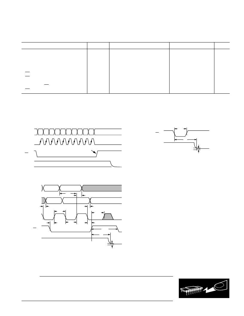
Figure 1a. Timing Diagram
±
1 % ERROR BAND
±
1 %
t
CSH
t
CSS
t
DH
Ax OR Dx
Ax OR Dx
t
PD_MIN
t
PD_MAX
A'x OR D'x
A'x OR D'x
1
0
1
0
1
0
V
DD
0V
SDI
(DATA IN)
CLK
CS
V
OUT
1
0
SDO
(DATA OUT)
t
DS
t
CH
t
CS1
t
CL
t
S
t
CSW
Figure 1b. Detail Timing Diagram
±
1%
±
1% ERROR BAND
RS
1
0
V
DD
V
DD
/2
V
OUT
t
RS
t
S
Figure 1c. Reset Timing Diagram
–5–
REV. B
ABSOLUTE MAXIMUM RATINGS*
(T
A
= +25
°
C, unless otherwise noted)
V
DD
to GND . . . . . . . . . . . . . . . . . . . . . . . . . . . . –0.3 V, +8 V
V
A
, V
B
, V
W
to GND . . . . . . . . . . . . . . . . . . . . . . . . . . 0 V, V
DD
A
X
–B
X
, A
X
–W
X
, B
X
–W
X
. . . . . . . . . . . . . . . . . . . . . .
±
20 mA
Digital Input and Output Voltage to GND . . . . . . . 0 V, +8 V
Operating Temperature Range . . . . . . . . . . . . –40
°
C to +85
°
C
Maximum Junction Temperature (T
J
max) . . . . . . . . . +150
°
C
Storage Temperature . . . . . . . . . . . . . . . . . . –65
°
C to +150
°
C
Lead Temperature (Soldering, 10 sec) . . . . . . . . . . . . . +300
°
C
Package Power Dissipation . . . . . . . . . . . . . . (T
J
max–T
A
)/
θ
JA
Thermal Resistance
(θ
JA
)
P-DIP (N-14) . . . . . . . . . . . . . . . . . . . . . . . . . . . . +83
°
C/W
P-DIP (N-24) . . . . . . . . . . . . . . . . . . . . . . . . . . . . +63
°
C/W
SOIC (SO-14) . . . . . . . . . . . . . . . . . . . . . . . . . . . +70
°
C/W
SOIC (SOL-24) . . . . . . . . . . . . . . . . . . . . . . . . . +120
°
C/W
TSSOP-14 (RU-14) . . . . . . . . . . . . . . . . . . . . . . +180
°
C/W
TSSOP-24 (RU-24) . . . . . . . . . . . . . . . . . . . . . . +143
°
C/W
*Stresses above those listed under “Absolute Maximum Ratings” may cause
permanent damage to the device. This is a stress rating only; functional operation
of the device at these or any other conditions above those listed in the operational
sections of this specification is not implied. Exposure to absolute maximum rating
conditions for extended periods may affect device reliability.
相關PDF資料 |
PDF描述 |
|---|---|
| AD841JN | Wideband, Unity-Gain Stable, Fast Settling Op Amp |
| AD841JCHIPS | Wideband, Unity-Gain Stable, Fast Settling Op Amp |
| AD841JH | Wideband, Unity-Gain Stable, Fast Settling Op Amp |
| AD841KH | Wideband, Unity-Gain Stable, Fast Settling Op Amp |
| AD841KN | Wideband, Unity-Gain Stable, Fast Settling Op Amp |
相關代理商/技術參數 |
參數描述 |
|---|---|
| AD84030001RR | 制造商:Rochester Electronics LLC 功能描述:- Bulk |
| AD84030005RUR | 制造商:Rochester Electronics LLC 功能描述:- Bulk |
| AD8403A10 | 制造商:Analog Devices 功能描述: |
| AD8403AN1 | 制造商:Rochester Electronics LLC 功能描述:QUAD 8-BIT POTENTIOMETER 1 OHM - Bulk |
| AD8403AN10 | 功能描述:IC POT DIG QUAD 10K 8BIT 24DIP RoHS:否 類別:集成電路 (IC) >> 數據采集 - 數字電位器 系列:- 標準包裝:3,000 系列:DPP 接片:32 電阻(歐姆):10k 電路數:1 溫度系數:標準值 300 ppm/°C 存儲器類型:非易失 接口:3 線串行(芯片選擇,遞增,增/減) 電源電壓:2.5 V ~ 6 V 工作溫度:-40°C ~ 85°C 安裝類型:表面貼裝 封裝/外殼:8-WFDFN 裸露焊盤 供應商設備封裝:8-TDFN(2x3) 包裝:帶卷 (TR) |
發布緊急采購,3分鐘左右您將得到回復。