- 您現(xiàn)在的位置:買(mǎi)賣(mài)IC網(wǎng) > PDF目錄373949 > AD8551ARM-REEL (ANALOG DEVICES INC) Zero-Drift, Single-Supply, Rail-to-Rail Input/Output Operational Amplifiers PDF資料下載
參數(shù)資料
| 型號(hào): | AD8551ARM-REEL |
| 廠(chǎng)商: | ANALOG DEVICES INC |
| 元件分類(lèi): | 運(yùn)動(dòng)控制電子 |
| 英文描述: | Zero-Drift, Single-Supply, Rail-to-Rail Input/Output Operational Amplifiers |
| 中文描述: | OP-AMP, 10 uV OFFSET-MAX, 1.5 MHz BAND WIDTH, PDSO8 |
| 封裝: | MO-187AA, MSOP-8 |
| 文件頁(yè)數(shù): | 18/24頁(yè) |
| 文件大小: | 416K |
| 代理商: | AD8551ARM-REEL |
第1頁(yè)第2頁(yè)第3頁(yè)第4頁(yè)第5頁(yè)第6頁(yè)第7頁(yè)第8頁(yè)第9頁(yè)第10頁(yè)第11頁(yè)第12頁(yè)第13頁(yè)第14頁(yè)第15頁(yè)第16頁(yè)第17頁(yè)當(dāng)前第18頁(yè)第19頁(yè)第20頁(yè)第21頁(yè)第22頁(yè)第23頁(yè)第24頁(yè)
AD8551/AD8552/AD8554
Rev. C | Page 18 of 24
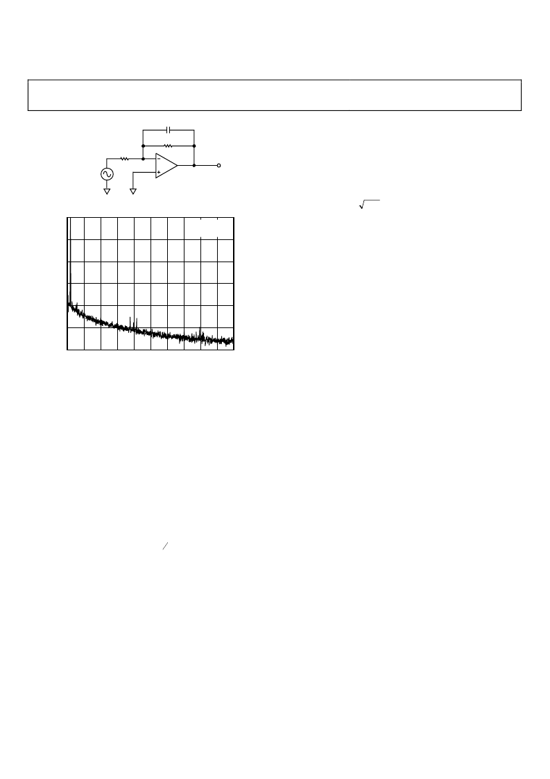
100
100k
3.3nF
V
IN
= 1mV rms
@ 200Hz
0
Figure 59. Reducing Autocorrection Clock Noise Using a Feedback Capacitor
FREQUENCY (kHz)
0
0
1
O
–20
–40
–60
–80
–100
–120
2
3
4
5
6
7
8
9
10
V
SY
= 5V
A
V
= 60dB
0
Figure 60. Spectral Analysis Using a Feedback Capacitor
BROADBAND AND EXTERNAL RESISTOR NOISE
CONSIDERATIONS
The total broadband noise output from any amplifier is primarily
a function of three types of noise: input voltage noise from the
amplifier, input current noise from the amplifier, and Johnson
noise from the external resistors used around the amplifier.
Input voltage noise, or e
n
, is strictly a function of the amplifier
used. The Johnson noise from a resistor is a function of the re-
sistance and the temperature. Input current noise, or i
n
, creates
an equivalent voltage noise proportional to the resistors used
around the amplifier. These noise sources are not correlated
with each other and their combined noise sums in a root-
squared-sum fashion. The full equation is given as
(
_
4
n
S
n
TOTAL
n
i
kTr
e
e
)
[
]
2
1
2
2
S
R
+
+
=
(15)
Where:
e
n
= the input voltage noise density of the amplifier.
i
n
= the input current noise of the amplifier.
R
S
= source resistance connected to the noninverting terminal.
k
= Boltzmann’s constant (1.38 × 10
23
J/K).
T
= ambient temperature in Kelvin (K = 273.15 + °C).
The input voltage noise density (e
n
) of the AD855x is 42 nV/√Hz,
and the input noise, i
n
, is 2 fA/√Hz. The e
n, TOTAL
is dominated by
the input voltage noise, provided the source resistance is less
than 106 kΩ. With source resistance greater than 106 kΩ, the
overall noise of the system is dominated by the Johnson noise of
the resistor itself.
Because the input current noise of the AD855x is very small,
it does not become a dominant term unless R
S
is greater than
4 GΩ, which is an impractical value of source resistance.
The total noise (e
n, TOTAL
) is expressed in volts per square root
Hertz, and the equivalent rms noise over a certain bandwidth
can be found as
BW
e
e
TOTAL
,
n
n
×
=
(16)
where
BW
is the bandwidth of interest in Hertz.
OUTPUT OVERDRIVE RECOVERY
The AD855x amplifiers have an excellent overdrive recovery of
only 200 μs from either supply rail. This characteristic is par-
ticularly difficult for autocorrection amplifiers because the
nulling amplifier requires a nontrivial amount of time to error
correct the main amplifier back to a valid output. Figure 29 and
Figure 30 show the positive and negative overdrive recovery
times for the AD855x.
The output overdrive recovery for an autocorrection amplifier is
defined as the time it takes for the output to correct to its final
voltage from an overload state. It is measured by placing the
amplifier in a high gain configuration with an input signal that
forces the output voltage to the supply rail. The input voltage is
then stepped down to the linear region of the amplifier, usually
to halfway between the supplies. The time from the input signal
stepdown to the output settling to within 100 μV of its final
value is the overdrive recovery time.
INPUT OVERVOLTAGE PROTECTION
Although the AD855x is a rail-to-rail input amplifier, exercise
care to ensure that the potential difference between the inputs
does not exceed 5 V. Under normal operating conditions, the
amplifier corrects its output to ensure the two inputs are at the
same voltage. However, if the device is configured as a comparator,
or is under some unusual operating condition, the input voltages
may be forced to different potentials. This can cause excessive
current to flow through internal diodes in the AD855x used to
protect the input stage against overvoltage.
If either input exceeds either supply rail by more than 0.3 V,
large amounts of current begin to flow through the ESD pro-
tection diodes in the amplifier. These diodes connect between
the inputs and each supply rail to protect the input transistors
against an electrostatic discharge event and are normally
reverse-biased. However, if the input voltage exceeds the supply
voltage, these ESD diodes become forward-biased. Without
current limiting, excessive amounts of current can flow through
these diodes, causing permanent damage to the device. If inputs
are subjected to overvoltage, appropriate series resistors should
be inserted to limit the diode current to less than 2 mA maximum.
相關(guān)PDF資料 |
PDF描述 |
|---|---|
| AD8551ARMZ-R2 | Zero-Drift, Single-Supply, Rail-to-Rail Input/Output Operational Amplifiers |
| AD8551ARMZ-REEL | Zero-Drift, Single-Supply, Rail-to-Rail Input/Output Operational Amplifiers |
| AD8551AR-REEL | Zero-Drift, Single-Supply, Rail-to-Rail Input/Output Operational Amplifiers |
| AD8551AR-REEL7 | Zero-Drift, Single-Supply, Rail-to-Rail Input/Output Operational Amplifiers |
| AD8551ARZ1 | Zero-Drift, Single-Supply, Rail-to-Rail Input/Output Operational Amplifiers |
相關(guān)代理商/技術(shù)參數(shù) |
參數(shù)描述 |
|---|---|
| AD8551ARMZ | 功能描述:IC OPAMP CHOPPER R-R 30MA 8MSOP RoHS:是 類(lèi)別:集成電路 (IC) >> Linear - Amplifiers - Instrumentation 系列:- 標(biāo)準(zhǔn)包裝:1 系列:- 放大器類(lèi)型:通用 電路數(shù):4 輸出類(lèi)型:滿(mǎn)擺幅 轉(zhuǎn)換速率:0.6 V/µs 增益帶寬積:1MHz -3db帶寬:- 電流 - 輸入偏壓:2pA 電壓 - 輸入偏移:1000µV 電流 - 電源:85µA 電流 - 輸出 / 通道:20mA 電壓 - 電源,單路/雙路(±):1.8 V ~ 6 V 工作溫度:-40°C ~ 125°C 安裝類(lèi)型:表面貼裝 封裝/外殼:14-SOIC(0.154",3.90mm 寬) 供應(yīng)商設(shè)備封裝:14-SOICN 包裝:剪切帶 (CT) 產(chǎn)品目錄頁(yè)面:680 (CN2011-ZH PDF) 其它名稱(chēng):MCP6L04T-E/SLCT |
| AD8551ARMZ-R2 | 制造商:Analog Devices 功能描述:SP Amp Zero Drift Amplifier Single R-R I/O 5V 8-Pin MSOP T/R 制造商:Analog Devices 功能描述:Operational Amplifier (Op-Amp) IC 制造商:Analog Devices 功能描述:IC OP AMP R/R SINGLE 8MSOP |
| AD8551ARMZ-REEL | 功能描述:IC OPAMP CHOPPER R-R 30MA 8MSOP RoHS:是 類(lèi)別:集成電路 (IC) >> Linear - Amplifiers - Instrumentation 系列:- 產(chǎn)品培訓(xùn)模塊:Differential Circuit Design Techniques for Communication Applications 標(biāo)準(zhǔn)包裝:1 系列:- 放大器類(lèi)型:RF/IF 差分 電路數(shù):1 輸出類(lèi)型:差分 轉(zhuǎn)換速率:9800 V/µs 增益帶寬積:- -3db帶寬:2.9GHz 電流 - 輸入偏壓:3µA 電壓 - 輸入偏移:- 電流 - 電源:40mA 電流 - 輸出 / 通道:- 電壓 - 電源,單路/雙路(±):3 V ~ 3.6 V 工作溫度:-40°C ~ 85°C 安裝類(lèi)型:表面貼裝 封裝/外殼:16-VQFN 裸露焊盤(pán),CSP 供應(yīng)商設(shè)備封裝:16-LFCSP-VQ 包裝:剪切帶 (CT) 產(chǎn)品目錄頁(yè)面:551 (CN2011-ZH PDF) 其它名稱(chēng):ADL5561ACPZ-R7CT |
| AD8551AR-REEL | 制造商:Analog Devices 功能描述:SP Amp Zero Drift Amplifier Single R-R I/O 5V 8-Pin SOIC N T/R |
| AD8551AR-REEL7 | 制造商:Analog Devices 功能描述:SP Amp Zero Drift Amplifier Single R-R I/O 5V 8-Pin SOIC N T/R |
發(fā)布緊急采購(gòu),3分鐘左右您將得到回復(fù)。