- 您現(xiàn)在的位置:買賣IC網(wǎng) > PDF目錄373949 > AD8551ARZ-REEL7 (ANALOG DEVICES INC) Zero-Drift, Single-Supply, Rail-to-Rail Input/Output Operational Amplifiers PDF資料下載
參數(shù)資料
| 型號(hào): | AD8551ARZ-REEL7 |
| 廠商: | ANALOG DEVICES INC |
| 元件分類: | 運(yùn)動(dòng)控制電子 |
| 英文描述: | Zero-Drift, Single-Supply, Rail-to-Rail Input/Output Operational Amplifiers |
| 中文描述: | OP-AMP, 10 uV OFFSET-MAX, 1.5 MHz BAND WIDTH, PDSO8 |
| 封裝: | ROHS COMPLIANT, MS-012AA, SOIC-8 |
| 文件頁數(shù): | 16/24頁 |
| 文件大小: | 416K |
| 代理商: | AD8551ARZ-REEL7 |
AD8551/AD8552/AD8554
earn the reputation of being among the most precise amplifiers
available on the market.
Rev. C | Page 16 of 24
HIGH GAIN, CMRR, PSRR
Common-mode and power supply rejection are indications
of the amount of offset voltage an amplifier has as a result of a
change in its input common-mode or power supply voltages. As
shown in the previous section, the autocorrection architecture
of the AD855x allows it to quite effectively minimize offset volt-
ages. The technique also corrects for offset errors caused by
common-mode voltage swings and power supply variations.
This results in superb CMRR and PSRR figures in excess of
130 dB. Because the autocorrection occurs continuously, these
figures can be maintained across the entire temperature range
of the device, from 40°C to +125°C.
MAXIMIZING PERFORMANCE THROUGH
PROPER LAYOUT
To achieve the maximum performance of the extremely high
input impedance and low offset voltage of the AD855x, care is
needed in laying out the circuit board. The PC board surface
must remain clean and free of moisture to avoid leakage cur-
rents between adjacent traces. Surface coating of the circuit
board reduces surface moisture and provides a humidity barrier,
reducing parasitic resistance on the board. The use of guard
rings around the amplifier inputs further reduces leakage cur-
rents. Figure 52 shows proper guard ring configuration, and
Figure 53 shows the top view of a surface-mount layout. The
guard ring does not need to be a specific width, but it should
form a continuous loop around both inputs. By setting the
guard ring voltage equal to the voltage at the noninverting
input, parasitic capacitance is minimized as well. For further
reduction of leakage currents, components can be mounted to
the PC board using Teflon standoff insulators.
AD8552
AD8552
AD8552
V
OUT
V
OUT
V
OUT
V
IN
V
IN
V
IN
0
Figure 52. Guard Ring Layout and Connections to Reduce
PC Board Leakage Currents
V+
AD8552
V–
R
2
R
1
R
1
R
2
V
REF
V
REF
V
IN2
GUARD
RING
GUARD
RING
V
IN1
0
Figure 53. Top View of AD8552 SOIC Layout with Guard Rings
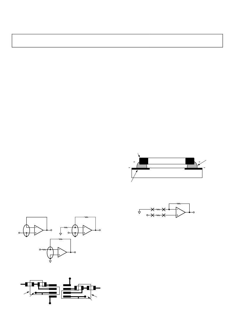
Other potential sources of offset error are thermoelectric
voltages on the circuit board. This voltage, also called Seebeck
voltage, occurs at the junction of two dissimilar metals and is
proportional to the temperature of the junction. The most
common metallic junctions on a circuit board are solder-to-
board trace and solder-to-component lead. Figure 54 shows a
cross-section of the thermal voltage error sources. If the
temperature of the PC board at one end of the component (T
A1
)
is different from the temperature at the other end (T
A2
), the
resulting Seebeck voltages are not equal, resulting in a thermal
voltage error.
This thermocouple error can be reduced by using dummy
components to match the thermoelectric error source. Placing
the dummy component as close as possible to its partner ensures
both Seebeck voltages are equal, thus canceling the thermo-
couple error. Maintaining a constant ambient temperature on
the circuit board further reduces this error. The use of a ground
plane helps distribute heat throughout the board and reduces
EMI noise pickup.
SOLDER
+
+
+
+
COMPONENT
LEAD
COPPER
TRACE
V
SC1
V
TS1
T
A1
SURFACE-MOUNT
COMPONENT
PC BOARD
T
A2
V
SC2
V
TS2
IF T
A1
≠
T
A2
, THEN
V
TS1
+ V
SC1
≠
V
TS2
+ V
SC2
0
Figure 54. Mismatch in Seebeck Voltages Causes
Thermoelectric Voltage Error
AD8551/
AD8552/
AD8554
A
V
= 1 + (R
F
/R
1
)
NOTES
1. R
S
SHOULD BE PLACED IN CLOSE PROXIMITY AND
ALIGNMENT TO R
1
TO BALANCE SEEBECK VOLTAGES.
R
S
= R
1
R
1
R
F
V
IN
V
OUT
0
Figure 55. Using Dummy Components to Cancel
Thermoelectric Voltage Errors
1/f NOISE CHARACTERISTICS
Another advantage of auto-zero amplifiers is their ability to
cancel flicker noise. Flicker noise, also known as 1/f noise, is
noise inherent in the physics of semiconductor devices, and it
increases 3 dB for every octave decrease in frequency. The 1/f
corner frequency of an amplifier is the frequency at which the
flicker noise is equal to the broadband noise of the amplifier.
At lower frequencies, flicker noise dominates, causing higher
degrees of error for sub-Hertz frequencies or dc precision
applications.
相關(guān)PDF資料 |
PDF描述 |
|---|---|
| AD8552AR-REEL | Zero-Drift, Single-Supply, Rail-to-Rail Input/Output Operational Amplifiers |
| AD8552AR-REEL7 | Zero-Drift, Single-Supply, Rail-to-Rail Input/Output Operational Amplifiers |
| AD8552ARU-REEL | Zero-Drift, Single-Supply, Rail-to-Rail Input/Output Operational Amplifiers |
| AD8552ARUZ1 | Zero-Drift, Single-Supply, Rail-to-Rail Input/Output Operational Amplifiers |
| AD8552ARUZ-REEL | Zero-Drift, Single-Supply, Rail-to-Rail Input/Output Operational Amplifiers |
相關(guān)代理商/技術(shù)參數(shù) |
參數(shù)描述 |
|---|---|
| AD8552 | 制造商:AD 制造商全稱:Analog Devices 功能描述:Zero-Drift, Single-Supply, Rail-to-Rail Input/Output Operational Amplifiers |
| AD8552AR | 功能描述:IC OPAMP CHOPPER R-R DUAL 8SOIC RoHS:否 類別:集成電路 (IC) >> Linear - Amplifiers - Instrumentation 系列:- 標(biāo)準(zhǔn)包裝:73 系列:Over-The-Top® 放大器類型:通用 電路數(shù):4 輸出類型:滿擺幅 轉(zhuǎn)換速率:0.07 V/µs 增益帶寬積:200kHz -3db帶寬:- 電流 - 輸入偏壓:1nA 電壓 - 輸入偏移:285µV 電流 - 電源:50µA 電流 - 輸出 / 通道:25mA 電壓 - 電源,單路/雙路(±):2 V ~ 44 V,±1 V ~ 22 V 工作溫度:-40°C ~ 85°C 安裝類型:表面貼裝 封裝/外殼:16-WFDFN 裸露焊盤 供應(yīng)商設(shè)備封裝:16-DFN-EP(5x3) 包裝:管件 |
| AD8552AR-REEL | 功能描述:IC OPAMP CHOPPER R-R DUAL 8SOIC RoHS:否 類別:集成電路 (IC) >> Linear - Amplifiers - Instrumentation 系列:- 標(biāo)準(zhǔn)包裝:50 系列:LinCMOS™ 放大器類型:通用 電路數(shù):4 輸出類型:- 轉(zhuǎn)換速率:0.05 V/µs 增益帶寬積:110kHz -3db帶寬:- 電流 - 輸入偏壓:0.7pA 電壓 - 輸入偏移:210µV 電流 - 電源:57µA 電流 - 輸出 / 通道:30mA 電壓 - 電源,單路/雙路(±):3 V ~ 16 V,±1.5 V ~ 8 V 工作溫度:-40°C ~ 85°C 安裝類型:表面貼裝 封裝/外殼:14-SOIC(0.154",3.90mm 寬) 供應(yīng)商設(shè)備封裝:14-SOIC 包裝:管件 產(chǎn)品目錄頁面:865 (CN2011-ZH PDF) 其它名稱:296-1834296-1834-5 |
| AD8552AR-REEL7 | 功能描述:IC OPAMP CHOPPER R-R DUAL 8SOIC RoHS:否 類別:集成電路 (IC) >> Linear - Amplifiers - Instrumentation 系列:- 其它有關(guān)文件:Automotive Product Guide 產(chǎn)品培訓(xùn)模塊:Lead (SnPb) Finish for COTS Obsolescence Mitigation Program 標(biāo)準(zhǔn)包裝:1 系列:- 放大器類型:通用 電路數(shù):1 輸出類型:滿擺幅 轉(zhuǎn)換速率:3 V/µs 增益帶寬積:10MHz -3db帶寬:- 電流 - 輸入偏壓:1pA 電壓 - 輸入偏移:70µV 電流 - 電源:2.5mA 電流 - 輸出 / 通道:48mA 電壓 - 電源,單路/雙路(±):2.7 V ~ 5.5 V,±1.35 V ~ 2.75 V 工作溫度:-40°C ~ 125°C 安裝類型:表面貼裝 封裝/外殼:SOT-23-6 供應(yīng)商設(shè)備封裝:SOT-6 包裝:Digi-Reel® 其它名稱:MAX4475AUT#TG16DKR |
| AD8552ARU | 功能描述:IC OPAMP CHOPPER R-R DUAL 8TSSOP RoHS:否 類別:集成電路 (IC) >> Linear - Amplifiers - Instrumentation 系列:- 標(biāo)準(zhǔn)包裝:73 系列:Over-The-Top® 放大器類型:通用 電路數(shù):4 輸出類型:滿擺幅 轉(zhuǎn)換速率:0.07 V/µs 增益帶寬積:200kHz -3db帶寬:- 電流 - 輸入偏壓:1nA 電壓 - 輸入偏移:285µV 電流 - 電源:50µA 電流 - 輸出 / 通道:25mA 電壓 - 電源,單路/雙路(±):2 V ~ 44 V,±1 V ~ 22 V 工作溫度:-40°C ~ 85°C 安裝類型:表面貼裝 封裝/外殼:16-WFDFN 裸露焊盤 供應(yīng)商設(shè)備封裝:16-DFN-EP(5x3) 包裝:管件 |
發(fā)布緊急采購,3分鐘左右您將得到回復(fù)。