- 您現在的位置:買賣IC網 > PDF目錄373949 > AD8554AR (ANALOG DEVICES INC) Zero-Drift, Single-Supply, Rail-to-Rail Input/Output Operational Amplifiers PDF資料下載
參數資料
| 型號: | AD8554AR |
| 廠商: | ANALOG DEVICES INC |
| 元件分類: | 運動控制電子 |
| 英文描述: | Zero-Drift, Single-Supply, Rail-to-Rail Input/Output Operational Amplifiers |
| 中文描述: | QUAD OP-AMP, 10 uV OFFSET-MAX, 1.5 MHz BAND WIDTH, PDSO14 |
| 封裝: | MS-012AB, SOIC-14 |
| 文件頁數: | 17/20頁 |
| 文件大小: | 262K |
| 代理商: | AD8554AR |
AD8551/AD8552/AD8554
–17–
REV. 0
Figure 62 shows the low-side monitor equivalent. In this circuit,
the input common-mode voltage to the AD8552 will be at or near
ground. Again, a 0.1
resistor provides a voltage drop propor-
tional to the return current. The output voltage is given as:
V
V
R
R
R
I
OUT
SENSE
L
=
+
×
×
2
1
(24)
For the component values shown in Figure 62, the output trans-
fer function decreases from V+ at –2.5 V/A.
8
1
4
3
+3V
0.1
m
F
R
SENSE
0.1
V
V+
I
L
G
S
D
2
M1
Si9433
MONITOR
OUTPUT
+3V
R
2.49k
V
R
1
100
V
1/2
AD8552
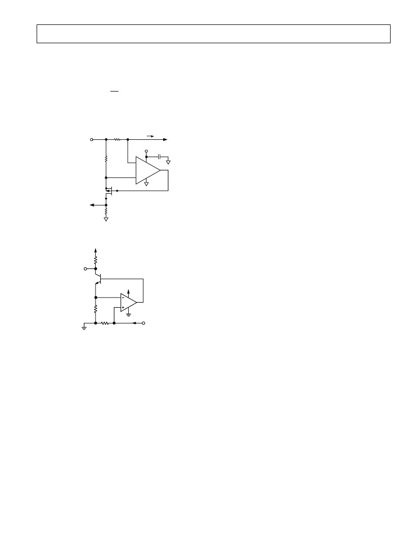
Figure 61. A High-Side Load Current Monitor
V+
RETURN TO
GROUND
1/2 AD8552
V+
R
2.49k
V
V
OUT
R
1
100
V
0.1
V
R
SENSE
Q1
Figure 62. A Low-Side Load Current Monitor
Precision Voltage Comparator
The AD855x can be operated open-loop and used as a precision
comparator. The AD855x has less than 50
μ
V of offset voltage
when run in this configuration. The slight increase of offset
voltage stems from the fact that the autocorrection architecture
operates with lowest offset in a closed loop configuration, that
is, one with negative feedback. With 50 mV of overdrive, the de-
vice has a propagation delay of 15
μ
s on the rising edge and
8
μ
s on the falling edge.
Care should be taken to ensure the maximum differential volt-
age of the device is not exceeded. For more information, please
refer to the section on Input Overvoltage Protection.
SPICE Model
The SPICE macro-model for the AD855x amplifier is given in
Listing 1. This model simulates the typical specifications for the
AD855x, and it can be downloaded from the Analog Devices
website at
http://www.analog.com.
The schematic of the
macro-model is shown in Figure 63.
Transistors M1 through M4 simulate the rail-to-rail input differ-
ential pairs in the AD855x amplifier. The EOS voltage source in
series with the noninverting input establishes not only the 1
μ
V
offset voltage, but is also used to establish common-mode and
power supply rejection ratios and input voltage noise. The dif-
ferential voltages from nodes 14 to 16 and nodes 17 to 18 are
reflected to E1, which is used to simulate a secondary pole-zero
combination in the open-loop gain of the amplifier.
The voltage at node 32 is then reflected to G1, which adds an
additional gain stage and, in conjunction with CF, establishes
the slew rate of the model at 0.5 V/
μ
s. M5 and M6 are in a
common-source configuration, similar to the output stage of the
AD855x amplifier. EG1 and EG2 fix the quiescent current in
these two transistors at 100
μ
A, and also help accurately simu-
late the V
OUT
vs. I
OUT
characteristic of the amplifier.
The network around ECM1 creates the common-mode voltage
error, with CCM1 setting the corner frequency for the CMRR
roll-off. The power supply rejection error is created by the
network around EPS1, with CPS3 establishing the corner fre-
quency for the PSRR roll-off. The two current loops around
nodes 80 and 81 are used to create a 42 nV/
√
Hz
noise figure
across RN2. All three of these error sources are reflected to the
input of the op amp model through EOS. Finally, GSY is used
to accurately model the supply current versus supply voltage in-
crease in the AD855x.
This macro-model has been designed to accurately simulate a
number of specifications exhibited by the AD855x amplifier,
and is one of the most true-to-life macro-models available for
any op amp. It is optimized for operation at +27
°
C. Although
the model will function at different temperatures, it may lose
accuracy with respect to the actual behavior of the AD855x.
相關PDF資料 |
PDF描述 |
|---|---|
| AD8554ARZ-REEL | Zero-Drift, Single-Supply, Rail-to-Rail Input/Output Operational Amplifiers |
| AD8551ARM-R2 | Zero-Drift, Single-Supply, Rail-to-Rail Input/Output Operational Amplifiers |
| AD8551ARM-REEL | Zero-Drift, Single-Supply, Rail-to-Rail Input/Output Operational Amplifiers |
| AD8551ARMZ-R2 | Zero-Drift, Single-Supply, Rail-to-Rail Input/Output Operational Amplifiers |
| AD8551ARMZ-REEL | Zero-Drift, Single-Supply, Rail-to-Rail Input/Output Operational Amplifiers |
相關代理商/技術參數 |
參數描述 |
|---|---|
| AD8554AR-REEL | 功能描述:IC OPAMP CHOPPER R-R QUAD 14SOIC RoHS:否 類別:集成電路 (IC) >> Linear - Amplifiers - Instrumentation 系列:- 標準包裝:2,500 系列:- 放大器類型:通用 電路數:1 輸出類型:滿擺幅 轉換速率:0.11 V/µs 增益帶寬積:350kHz -3db帶寬:- 電流 - 輸入偏壓:4nA 電壓 - 輸入偏移:20µV 電流 - 電源:260µA 電流 - 輸出 / 通道:20mA 電壓 - 電源,單路/雙路(±):2.7 V ~ 36 V,±1.35 V ~ 18 V 工作溫度:-40°C ~ 85°C 安裝類型:表面貼裝 封裝/外殼:8-SOIC(0.154",3.90mm 寬) 供應商設備封裝:8-SO 包裝:帶卷 (TR) |
| AD8554AR-REEL7 | 功能描述:IC OPAMP CHOPPER R-R QUAD 14SOIC RoHS:否 類別:集成電路 (IC) >> Linear - Amplifiers - Instrumentation 系列:- 標準包裝:2,500 系列:- 放大器類型:通用 電路數:1 輸出類型:滿擺幅 轉換速率:0.11 V/µs 增益帶寬積:350kHz -3db帶寬:- 電流 - 輸入偏壓:4nA 電壓 - 輸入偏移:20µV 電流 - 電源:260µA 電流 - 輸出 / 通道:20mA 電壓 - 電源,單路/雙路(±):2.7 V ~ 36 V,±1.35 V ~ 18 V 工作溫度:-40°C ~ 85°C 安裝類型:表面貼裝 封裝/外殼:8-SOIC(0.154",3.90mm 寬) 供應商設備封裝:8-SO 包裝:帶卷 (TR) |
| AD8554ARU | 制造商:Analog Devices 功能描述:SP Amp Zero Drift Amplifier Quad R-R I/O 5V 14-Pin TSSOP 制造商:Rochester Electronics LLC 功能描述:QUAD PRECISION RAIL-RAIL CHOPPER OP AMP - Bulk 制造商:Analog Devices 功能描述:IC OP-AMP QUAD R/R |
| AD8554ARU-REEL | 制造商:Analog Devices 功能描述:SP Amp Zero Drift Amplifier Quad R-R I/O 5V 14-Pin TSSOP T/R 制造商:Rochester Electronics LLC 功能描述:QUAD PRECISION RAIL-RAIL CHOPPER OP AMP - Tape and Reel |
| AD8554ARUZ | 功能描述:IC OPAMP CHOPPER R-R 14TSSOP RoHS:是 類別:集成電路 (IC) >> Linear - Amplifiers - Instrumentation 系列:- 標準包裝:2,500 系列:- 放大器類型:通用 電路數:4 輸出類型:- 轉換速率:0.6 V/µs 增益帶寬積:1MHz -3db帶寬:- 電流 - 輸入偏壓:45nA 電壓 - 輸入偏移:2000µV 電流 - 電源:1.4mA 電流 - 輸出 / 通道:40mA 電壓 - 電源,單路/雙路(±):3 V ~ 32 V,±1.5 V ~ 16 V 工作溫度:0°C ~ 70°C 安裝類型:表面貼裝 封裝/外殼:14-TSSOP(0.173",4.40mm 寬) 供應商設備封裝:14-TSSOP 包裝:帶卷 (TR) 其它名稱:LM324ADTBR2G-NDLM324ADTBR2GOSTR |
發布緊急采購,3分鐘左右您將得到回復。