- 您現(xiàn)在的位置:買賣IC網(wǎng) > PDF目錄373949 > AD8554ARU (ANALOG DEVICES INC) Zero-Drift, Single-Supply, Rail-to-Rail Input/Output Operational Amplifiers PDF資料下載
參數(shù)資料
| 型號: | AD8554ARU |
| 廠商: | ANALOG DEVICES INC |
| 元件分類: | 運(yùn)動控制電子 |
| 英文描述: | Zero-Drift, Single-Supply, Rail-to-Rail Input/Output Operational Amplifiers |
| 中文描述: | QUAD OP-AMP, 10 uV OFFSET-MAX, 1.5 MHz BAND WIDTH, PDSO14 |
| 封裝: | MO-153AB-1, TSSOP-14 |
| 文件頁數(shù): | 10/20頁 |
| 文件大小: | 262K |
| 代理商: | AD8554ARU |
AD8551/AD8552/AD8554
–10–
REV. 0
FUNCTIONAL DESCRIPTION
The AD855x family of amplifiers are high precision rail-to-rail
operational amplifiers that can be run from a single supply volt-
age. Their typical offset voltage of less than 1
μ
V allows these
amplifiers to be easily configured for high gains without risk of
excessive output voltage errors. The extremely small tempera-
ture drift of 5 nV/
°
C ensures a minimum of offset voltage error
over its entire temperature range of –40
°
C to +125
°
C, making
the AD855x amplifiers ideal for a variety of sensitive measure-
ment applications in harsh operating environments such as
under-hood and braking/suspension systems in automobiles.
The AD855x family are CMOS amplifiers and achieve their
high degree of precision through autozero stabilization. This
autocorrection topology allows the AD855x to maintain its low
offset voltage over a wide temperature range and over its operat-
ing lifetime.
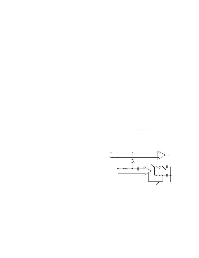
Amplifier Architecture
Each AD855x op amp consists of two amplifiers, a main amplifier
and a secondary amplifier, used to correct the offset voltage of the
main amplifier. Both consist of a rail-to-rail input stage, allowing
the input common-mode voltage range to reach both supply rails.
The input stage consists of an NMOS differential pair operating
concurrently with a parallel PMOS differential pair. The outputs
from the differential input stages are combined in another gain
stage whose output is used to drive a rail-to-rail output stage.
The wide voltage swing of the amplifier is achieved by using two
output transistors in a common-source configuration. The output
voltage range is limited by the drain to source resistance of these
transistors. As the amplifier is required to source or sink more
output current, the r
DS
of these transistors increases, raising the
voltage drop across these transistors. Simply put, the output volt-
age will not swing as close to the rail under heavy output current
conditions as it will with light output current. This is a character-
istic of all rail-to-rail output amplifiers. Figures 6 and 7 show how
close the output voltage can get to the rails with a given output
current. The output of the AD855x is short circuit protected to
approximately 50 mA of current.
The AD855x amplifiers have exceptional gain, yielding greater
than 120 dB of open-loop gain with a load of 2 k
. Because the
output transistors are configured in a common-source configu-
ration, the gain of the output stage, and thus the open-loop gain
of the amplifier, is dependent on the load resistance. Open-loop
gain will decrease with smaller load resistances. This is another
characteristic of rail-to-rail output amplifiers.
Basic Autozero Amplifier Theory
Autocorrection amplifiers are not a new technology. Various IC
implementations have been available for over 15 years and some
improvements have been made over time. The AD855x design
offers a number of significant performance improvements over
older versions while attaining a very substantial reduction in de-
vice cost. This section offers a simplified explanation of how the
AD855x is able to offer extremely low offset voltages and high
open-loop gains.
As noted in the previous section on amplifier architecture, each
AD855x op amp contains two internal amplifiers. One is used as
the primary amplifier, the other as an autocorrection, or nulling,
amplifier. Each amplifier has an associated input offset voltage,
which can be modeled as a dc voltage source in series with the
noninverting input. In Figures 44 and 45 these are labeled as
V
OSX
, where x denotes the amplifier associated with the offset; A
for the nulling amplifier, B for the primary amplifier. The open-
loop gain for the +IN and –IN inputs of each amplifier is given
as A
X
. Both amplifiers also have a third voltage input with an
associated open-loop gain of B
X
.
There are two modes of operation determined by the action of
two sets of switches in the amplifier: An autozero phase and an
amplification phase.
Autozero Phase
In this phase, all
φ
A switches are closed and all
φ
B switches are
opened. Here, the nulling amplifier is taken out of the gain loop
by shorting its two inputs together. Of course, there is a degree of
offset voltage, shown as
V
OSA
, inherent in the nulling amplifier
which maintains a potential difference between the +IN and –IN
inputs. The nulling amplifier feedback loop is closed through
φ
A
2
and V
OSA
appears at the output of the nulling amp and on C
M1
,
an internal capacitor in the AD855x. Mathematically, we can ex-
press this in the time domain as:
[ ]
=
which can be expressed as,
V
t
A V
t
B V
t
OA
[ ]
[ ]
(1)
V
t
A V
+
1
t
B
OA
A
[ ]
=
[ ]
(2)
This shows us that the offset voltage of the nulling amplifier
times a gain factor appears at the output of the nulling amplifier
and thus on the C
M1
capacitor.
V
IN+
V
IN
2
V
OUT
A
B
A
A
F
A
F
B
V
OSA
+
B
B
C
M2
C
M1
F
A
F
B
V
NB
V
NA
2
B
A
V
OA
Figure 44. Autozero Phase of the AD855x
Amplification Phase
When the
φ
B switches close and the
φ
A switches open for the
amplification phase, this offset voltage remains on C
M1
and
essentially corrects any error from the nulling amplifier. The
voltage across C
M1
is designated as V
NA
. Let us also designate
V
IN
as the potential difference between the two inputs to the
primary amplifier, or V
IN
= (V
IN+
– V
IN–
). Now the output of the
nulling amplifier can be expressed as:
[ ]
=
V
t
A V
t
V
t
B V
t
OA
IN
OSA
[ ]
[ ]
)
[ ]
(3)
相關(guān)PDF資料 |
PDF描述 |
|---|---|
| AD8551AR | Zero-Drift, Single-Supply, Rail-to-Rail Input/Output Operational Amplifiers |
| AD8551ARM | Zero-Drift, Single-Supply, Rail-to-Rail Input/Output Operational Amplifiers |
| AD8552AR | Zero-Drift, Single-Supply, Rail-to-Rail Input/Output Operational Amplifiers |
| AD8552ARU | Zero-Drift, Single-Supply, Rail-to-Rail Input/Output Operational Amplifiers |
| AD8554AR | Zero-Drift, Single-Supply, Rail-to-Rail Input/Output Operational Amplifiers |
相關(guān)代理商/技術(shù)參數(shù) |
參數(shù)描述 |
|---|---|
| AD8554ARU-REEL | 制造商:Analog Devices 功能描述:SP Amp Zero Drift Amplifier Quad R-R I/O 5V 14-Pin TSSOP T/R 制造商:Rochester Electronics LLC 功能描述:QUAD PRECISION RAIL-RAIL CHOPPER OP AMP - Tape and Reel |
| AD8554ARUZ | 功能描述:IC OPAMP CHOPPER R-R 14TSSOP RoHS:是 類別:集成電路 (IC) >> Linear - Amplifiers - Instrumentation 系列:- 標(biāo)準(zhǔn)包裝:2,500 系列:- 放大器類型:通用 電路數(shù):4 輸出類型:- 轉(zhuǎn)換速率:0.6 V/µs 增益帶寬積:1MHz -3db帶寬:- 電流 - 輸入偏壓:45nA 電壓 - 輸入偏移:2000µV 電流 - 電源:1.4mA 電流 - 輸出 / 通道:40mA 電壓 - 電源,單路/雙路(±):3 V ~ 32 V,±1.5 V ~ 16 V 工作溫度:0°C ~ 70°C 安裝類型:表面貼裝 封裝/外殼:14-TSSOP(0.173",4.40mm 寬) 供應(yīng)商設(shè)備封裝:14-TSSOP 包裝:帶卷 (TR) 其它名稱:LM324ADTBR2G-NDLM324ADTBR2GOSTR |
| AD8554ARUZ | 制造商:Analog Devices 功能描述:IC OP-AMP 1.5MHZ 制造商:Analog Devices 功能描述:IC, OP-AMP, 1.5MHZ, 0.4V/ us, TSSOP-14 |
| AD8554ARUZ | 制造商:Analog Devices 功能描述:IC OP AMP 1.5MHZ 0.4V/US 14TSSOP |
| AD8554ARUZ-REEL | 功能描述:IC OPAMP CHOPPER R-R 14TSSOP RoHS:是 類別:集成電路 (IC) >> Linear - Amplifiers - Instrumentation 系列:- 標(biāo)準(zhǔn)包裝:73 系列:Over-The-Top® 放大器類型:通用 電路數(shù):4 輸出類型:滿擺幅 轉(zhuǎn)換速率:0.07 V/µs 增益帶寬積:200kHz -3db帶寬:- 電流 - 輸入偏壓:1nA 電壓 - 輸入偏移:285µV 電流 - 電源:50µA 電流 - 輸出 / 通道:25mA 電壓 - 電源,單路/雙路(±):2 V ~ 44 V,±1 V ~ 22 V 工作溫度:-40°C ~ 85°C 安裝類型:表面貼裝 封裝/外殼:16-WFDFN 裸露焊盤 供應(yīng)商設(shè)備封裝:16-DFN-EP(5x3) 包裝:管件 |
發(fā)布緊急采購,3分鐘左右您將得到回復(fù)。