- 您現在的位置:買賣IC網 > PDF目錄373949 > AD8554ARZ1 (Analog Devices, Inc.) Zero-Drift, Single-Supply, Rail-to-Rail Input/Output Operational Amplifiers PDF資料下載
參數資料
| 型號: | AD8554ARZ1 |
| 廠商: | Analog Devices, Inc. |
| 英文描述: | Zero-Drift, Single-Supply, Rail-to-Rail Input/Output Operational Amplifiers |
| 中文描述: | 零漂移,單電源,軌到軌輸入/輸出運算放大器 |
| 文件頁數: | 15/24頁 |
| 文件大小: | 416K |
| 代理商: | AD8554ARZ1 |
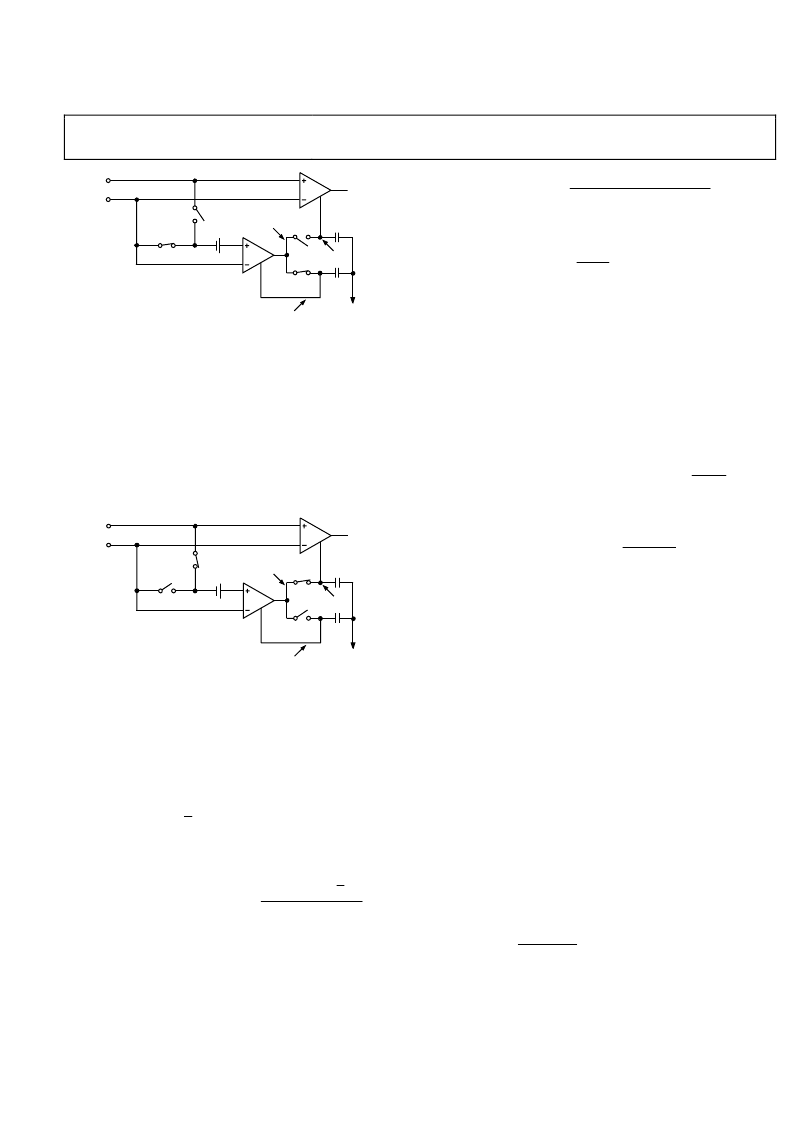
AD8551/AD8552/AD8554
Rev. C | Page 15 of 24
+
A
B
B
B
C
M2
V
IN+
V
NB
C
M1
V
OA
–B
A
V
NA
Ф
B
Ф
A
A
A
V
OSA
Ф
B
Ф
A
V
OUT
V
IN–
0
Figure 50. Auto-Zero Phase of the AD855x
Amplification Phase
When the φB switches close and the φA switches open for the
amplification phase, this offset voltage remains on C
M1
and,
essentially, corrects any error from the nulling amplifier. The
voltage across C
M1
is designated as V
NA
. Furthermore, V
IN
is
designated as the potential difference between the two inputs to
the primary amplifier, or V
IN
= (V
IN+
V
IN
). Thus, the nulling
amplifier can be expressed as
[ ]
[ ]
(
t
V
V
A
t
V
OSA
IN
A
OA
]
[
)
[ ]
t
V
B
NA
A
=
(3)
+
A
B
B
B
C
M2
V
IN+
V
NB
C
M1
V
OA
–B
A
V
NA
Ф
B
Ф
A
A
A
V
OSA
Ф
B
Ф
A
V
OUT
V
IN–
0
Figure 51. Output Phase of the Amplifier
Because φA is now open and there is no place for C
M1
to
discharge, the voltage (V
NA
), at the present time (t), is equal to
the voltage at the output of the nulling amp (V
OA
) at the time
when φA was closed. If the period of the autocorrection switching
frequency is labeled t
S
, then the amplifier switches between
phases every 0.5 × t
S
. Therefore, in the amplification phase
[ ]
t
=
S
NA
NA
t
V
V
2
1
(4)
Substituting Equation 4 and Equation 2 into Equation 3 yields
[ ]
[ ]
[ ]
t
A
S
OSA
A
A
OSA
A
IN
A
OA
B
t
V
B
A
V
A
V
A
V
+
+
=
1
2
1
(5)
For the sake of simplification, assume that the autocorrection
frequency is much faster than any potential change in V
OSA
or
V
OSB
. This is a valid assumption because changes in offset
voltage are a function of temperature variation or long-term
wear time, both of which are much slower than the auto-zero
clock frequency of the AD855x. This effectively renders V
time invariant; therefore, Equation 5 can be rearranged and
rewritten as
[ ]
t
[ ]
t
(
)
A
OSA
A
A
OSA
+
A
A
IN
A
OA
B
V
B
A
V
1
B
A
V
A
V
+
+
=
1
(6)
or
[ ]
t
[ ]
t
+
+
=
A
OSA
B
IN
A
OA
V
1
V
A
V
(7)
From these equations, the auto-zeroing action becomes evident.
Note the V
OS
term is reduced by a 1 + B
A
factor. This shows how
the nulling amplifier has greatly reduced its own offset voltage
error even before correcting the primary amplifier. This results
in the primary amplifier output voltage becoming the voltage at
the output of the AD855x amplifier. It is equal to
[ ]
[ ]
(
)
OSB
IN
B
OUT
V
V
A
V
NB
B
V
B
+
+
=
(8)
In the amplification phase, V
OA
= V
NB
, so this can be rewritten as
[ ]
t
[ ]
t
[ ]
t
+
+
+
+
=
A
OSB
B
IN
A
B
OSB
B
IN
B
OUT
V
V
A
B
V
A
V
A
V
1
(9)
Combining terms,
[ ]
t
[ ]
(
)
OSA
B
A
OSA
A
A
1
B
B
B
IN
OUT
V
V
A
B
V
B
+
A
B
A
A
V
+
+
+
=
(10)
The AD855x architecture is optimized in such a way that
A
A
=
A
B
and
B
A
=
B
OS
B
and
B
A
>> 1
Also, the gain product of A
A
B
B
B
is much greater than A
B
B
. These
allow Equation 10 to be simplified to
[ ]
[ ]
A
A
A
IN
OUT
A
B
A
t
V
t
V
(
)
OSB
OSA
V
V
+
+
≈
(11)
Most obvious is the gain product of both the primary and
nulling amplifiers. This A
A
B
B
A
term is what gives the AD855x its
extremely high open-loop gain. To understand how V
OSA
and
V
OSB
B
relate to the overall effective input offset voltage of the
complete amplifier, establish the generic amplifier equation of
(
EFF
OS
IN
OUT
V
V
k
V
,
)
+
×
=
(12)
where
k
is the open-loop gain of an amplifier and
V
OS, EFF
is its
effective offset voltage.
Putting Equation 12 into the form of Equation 11 gives
[ ]
[ ]
A
A
IN
OUT
B
A
V
V
A
A
EFF
OS
B
A
V
,
+
≈
(13)
Thus, it is evident that
A
OSB
OSA
EFF
OS
B
V
V
V
+
≈
,
(14)
The offset voltages of both the primary and nulling amplifiers
are reduced by the Gain Factor B
A
. This takes a typical input
offset voltage from several millivolts down to an effective input
offset voltage of submicrovolts. This autocorrection scheme is
the outstanding feature of the AD855x series that continues to
相關PDF資料 |
PDF描述 |
|---|---|
| AD8554ARZ-REEL7 | Zero-Drift, Single-Supply, Rail-to-Rail Input/Output Operational Amplifiers |
| AD8555AR-REEL | Zero-Drift, Digitally Programmable Sensor Signal Amplifier |
| AD8555ACP-REEL7 | Zero-Drift, Digitally Programmable Sensor Signal Amplifier |
| AD8555AR | Zero-Drift, Digitally Programmable Sensor Signal Amplifier |
| AD8555AR-REEL7 | Zero-Drift, Digitally Programmable Sensor Signal Amplifier |
相關代理商/技術參數 |
參數描述 |
|---|---|
| AD8554ARZ-REEL | 功能描述:IC OPAMP CHOPPER R-R QUAD 14SOIC RoHS:是 類別:集成電路 (IC) >> Linear - Amplifiers - Instrumentation 系列:- 標準包裝:73 系列:Over-The-Top® 放大器類型:通用 電路數:4 輸出類型:滿擺幅 轉換速率:0.07 V/µs 增益帶寬積:200kHz -3db帶寬:- 電流 - 輸入偏壓:1nA 電壓 - 輸入偏移:285µV 電流 - 電源:50µA 電流 - 輸出 / 通道:25mA 電壓 - 電源,單路/雙路(±):2 V ~ 44 V,±1 V ~ 22 V 工作溫度:-40°C ~ 85°C 安裝類型:表面貼裝 封裝/外殼:16-WFDFN 裸露焊盤 供應商設備封裝:16-DFN-EP(5x3) 包裝:管件 |
| AD8554ARZ-REEL7 | 功能描述:IC OPAMP CHOPPER R-R QUAD 14SOIC RoHS:是 類別:集成電路 (IC) >> Linear - Amplifiers - Instrumentation 系列:- 標準包裝:73 系列:Over-The-Top® 放大器類型:通用 電路數:4 輸出類型:滿擺幅 轉換速率:0.07 V/µs 增益帶寬積:200kHz -3db帶寬:- 電流 - 輸入偏壓:1nA 電壓 - 輸入偏移:285µV 電流 - 電源:50µA 電流 - 輸出 / 通道:25mA 電壓 - 電源,單路/雙路(±):2 V ~ 44 V,±1 V ~ 22 V 工作溫度:-40°C ~ 85°C 安裝類型:表面貼裝 封裝/外殼:16-WFDFN 裸露焊盤 供應商設備封裝:16-DFN-EP(5x3) 包裝:管件 |
| AD8555 | 制造商:AD 制造商全稱:Analog Devices 功能描述:Zero-Drift, Digitally Programmable Sensor Signal Amplifier |
| AD8555_09 | 制造商:AD 制造商全稱:Analog Devices 功能描述:Zero-Drift, Digitally Programmable Sensor Signal Amplifier |
| AD85551 | 制造商:AD 制造商全稱:Analog Devices 功能描述:10 MHz, 20 V/レs, G = 1, 10, 100, 1000 i CMOS㈢ Programmable Gain Instrumentation Amplifier |
發布緊急采購,3分鐘左右您將得到回復。