- 您現(xiàn)在的位置:買賣IC網(wǎng) > PDF目錄373950 > AD8582AN (ANALOG DEVICES INC) +5 Volt, Parallel Input Complete Dual 12-Bit DAC PDF資料下載
參數(shù)資料
| 型號(hào): | AD8582AN |
| 廠商: | ANALOG DEVICES INC |
| 元件分類: | DAC |
| 英文描述: | +5 Volt, Parallel Input Complete Dual 12-Bit DAC |
| 中文描述: | DUAL, PARALLEL, WORD INPUT LOADING, 16 us SETTLING TIME, 12-BIT DAC, PDIP24 |
| 封裝: | PLASTIC, DIP-24 |
| 文件頁(yè)數(shù): | 3/8頁(yè) |
| 文件大小: | 309K |
| 代理商: | AD8582AN |
–3–
REV. 0
AD8582
WARNING!
ESD SENSITIVE DEVICE
C AUT ION
ESD (electrostatic discharge) sensitive device. Electrostatic charges as high as 4000 V readily
accumulate on the human body and test equipment and can discharge without detection.
Although the AD8582 features proprietary ESD protection circuitry, permanent damage may
occur on devices subjected to high energy electrostatic discharges. T herefore, proper ESD
precautions are recommended to avoid performance degradation or loss of functionality.
ABSOLUT E MAX IMUM RAT INGS*
V
DD
to DGND & AGND . . . . . . . . . . . . . . . . . . . –0.3 V, +7 V
Logic Inputs to DGND . . . . . . . . . . . . . . .–0.3 V, V
DD
+ 0.3 V
V
OUT
to AGND . . . . . . . . . . . . . . . . . . . . .–0.3 V, V
DD
+ 0.3 V
V
REF
to AGND . . . . . . . . . . . . . . . . . . . . .–0.3 V, V
DD
+ 0.3 V
AGND to DGND . . . . . . . . . . . . . . . . . . . . . . . . . –0.3 V, V
DD
I
OUT
Short Circuit to GND . . . . . . . . . . . . . . . . . . . . . . 50 mA
Package Power Dissipation . . . . . . . . . . . . . . .(T
J
max–T
A
)/
θ
JA
T hermal Resistance,
θ
JA
24-Pin Plastic DIP Package (N-24) . . . . . . . . . . . . . 62
°
C/W
24-Lead SOIC Package (SOL-24) . . . . . . . . . . . . . . 73
°
C/W
Maximum Junction T emperature (T
J
max) . . . . . . . . . . 150
°
C
Operating T emperature Range . . . . . . . . . . . . .–40
°
C to +85
°
C
Storage T emperature Range . . . . . . . . . . . . .–65
°
C to +150
°
C
Lead T emperature (Soldering, 10 sec) . . . . . . . . . . . . . +300
°
C
*Stresses above those listed under “Absolute Maximum Ratings” may cause
permanent damage to the device. T his is a stress rating only and functional
operation of the device at these or any other conditions above those indicated in the
operational sections of this specification is not implied. Exposure to absolute
maximum rating conditions for extended periods may affect device reliability.
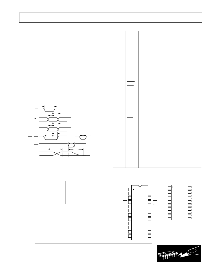
PIN DE SCRIPT ION
Pin No.
Name
Description
1, 24
V
OUT A
V
OUT B
Voltage outputs from the DACs. Fixed
output voltage range of 0 V to 4.095 V
with 1 mV/LSB. An internal
temperature stabilized reference
maintains a fixed full-scale voltage
independent of time, temperature and
power supply variations.
Analog Ground. Ground reference for
the internal bandgap reference voltage,
the DAC, and the output buffer.
Digital ground for input logic.
Load DAC register strobes. T ransfers
input register data to the DAC registers.
Active low inputs, Level sensitive latch.
May be connected together to double-
buffer load DAC registers.
Digital Input: High presets DAC
registers to half scale (800
H
), Low
clears DAC registers to zero (000
H
)
upon
RST
assertion.
Active low digital input that clears the
DAC register to zero, setting the DAC
to minimum scale when MSB pin = 0,
or half-scale when MSB pin = 1.
T welve Binary Data Bit Inputs. DB11 is
the MSB and DB0 is the LSB.
Chip Select. Active low input.
Select DAC A = 0 or DAC B = 1.
Positive Supply. Nominal value +5 V,
±
5%.
Nominal 2.5 V reference output
voltage. T his node must be buffered if
required to drive external loads.
2
AGND
3
4, 21
DGND
LDA,
LDB
5
MSB
6
RST
7–18
DB
0–11
19
20
22
23
CS
A
/B
V
DD
V
REF
PIN CONFIGURAT IONS
N-24
24-Pin Plastic DIP
SOL-24
24-Pin SOIC
V
OUTA
AGND
V
OUTB
V
REF
MSB
DB0
DB11
DGND
V
DD
DB1
DB10
DB2
DB9
DB3
DB8
DB4
DB7
DB5
DB6
14
1
2
24
23
5
6
7
20
19
18
3
4
22
21
8
17
9
16
10
15
11
TOP VIEW
(Not to Scale)
12
13
AD8582
LDA
RST
LDB
CS
A/B
TOP VIEW
(Not to Scale)
12
13
AD8582
1
24
LDA, LDB
CS
A/B
D0–D11
RST
t
AS
t
AH
t
DS
t
DH
t
LDW
t
RSW
t
LS
t
LH
V
OUT
t
S
t
S
± 1LSB
ERROR BAND
t
CSW
Timing Diagram
ORDE RING INFORMAT ION*
T emperature
Range
Package
Description
Package
Option
Model
AD8582AN
AD8582AR
AD8582Chips
–40
°
C to +85
°
C
–40
°
C to +85
°
C
+25
°
C
24-Pin Plastic DIP N-24
24-Lead SOIC
Die
SOL-24
*For die specifications contact your local Analog Devices sales office. T he
AD8582 contains 1270 transistors.
相關(guān)PDF資料 |
PDF描述 |
|---|---|
| AD8582AR | +5 Volt, Parallel Input Complete Dual 12-Bit DAC |
| AD8591 | CMOS Single Supply Rail-to-Rail Input/Output Operational Amplifiers with Shutdown |
| AD8591ART | CMOS Single Supply Rail-to-Rail Input/Output Operational Amplifiers with Shutdown |
| AD8592ARM | CMOS Single Supply Rail-to-Rail Input/Output Operational Amplifiers with Shutdown |
| AD8594AR | CMOS Single Supply Rail-to-Rail Input/Output Operational Amplifiers with Shutdown |
相關(guān)代理商/技術(shù)參數(shù) |
參數(shù)描述 |
|---|---|
| AD8582ANZ | 功能描述:IC DAC DUAL 12BIT 5V 24DIP RoHS:是 類別:集成電路 (IC) >> 數(shù)據(jù)采集 - 數(shù)模轉(zhuǎn)換器 系列:- 標(biāo)準(zhǔn)包裝:1 系列:- 設(shè)置時(shí)間:4.5µs 位數(shù):12 數(shù)據(jù)接口:串行,SPI? 轉(zhuǎn)換器數(shù)目:1 電壓電源:單電源 功率耗散(最大):- 工作溫度:-40°C ~ 125°C 安裝類型:表面貼裝 封裝/外殼:8-SOIC(0.154",3.90mm 寬) 供應(yīng)商設(shè)備封裝:8-SOICN 包裝:剪切帶 (CT) 輸出數(shù)目和類型:1 電壓,單極;1 電壓,雙極 采樣率(每秒):* 其它名稱:MCP4921T-E/SNCTMCP4921T-E/SNRCTMCP4921T-E/SNRCT-ND |
| AD8582AR | 功能描述:IC DAC 12BIT DUAL 5V 24-SOIC RoHS:否 類別:集成電路 (IC) >> 數(shù)據(jù)采集 - 數(shù)模轉(zhuǎn)換器 系列:- 產(chǎn)品培訓(xùn)模塊:Data Converter Fundamentals DAC Architectures 標(biāo)準(zhǔn)包裝:750 系列:- 設(shè)置時(shí)間:7µs 位數(shù):16 數(shù)據(jù)接口:并聯(lián) 轉(zhuǎn)換器數(shù)目:1 電壓電源:雙 ± 功率耗散(最大):100mW 工作溫度:0°C ~ 70°C 安裝類型:表面貼裝 封裝/外殼:28-LCC(J 形引線) 供應(yīng)商設(shè)備封裝:28-PLCC(11.51x11.51) 包裝:帶卷 (TR) 輸出數(shù)目和類型:1 電壓,單極;1 電壓,雙極 采樣率(每秒):143k |
| AD8582AR-REEL | 功能描述:IC DAC DUAL 12BIT 5V 24SOIC RoHS:否 類別:集成電路 (IC) >> 數(shù)據(jù)采集 - 數(shù)模轉(zhuǎn)換器 系列:- 產(chǎn)品培訓(xùn)模塊:Data Converter Fundamentals DAC Architectures 標(biāo)準(zhǔn)包裝:750 系列:- 設(shè)置時(shí)間:7µs 位數(shù):16 數(shù)據(jù)接口:并聯(lián) 轉(zhuǎn)換器數(shù)目:1 電壓電源:雙 ± 功率耗散(最大):100mW 工作溫度:0°C ~ 70°C 安裝類型:表面貼裝 封裝/外殼:28-LCC(J 形引線) 供應(yīng)商設(shè)備封裝:28-PLCC(11.51x11.51) 包裝:帶卷 (TR) 輸出數(shù)目和類型:1 電壓,單極;1 電壓,雙極 采樣率(每秒):143k |
| AD8582ARZ | 功能描述:IC DAC 12BIT DUAL 5V 24-SOIC RoHS:是 類別:集成電路 (IC) >> 數(shù)據(jù)采集 - 數(shù)模轉(zhuǎn)換器 系列:- 產(chǎn)品培訓(xùn)模塊:Lead (SnPb) Finish for COTS Obsolescence Mitigation Program 標(biāo)準(zhǔn)包裝:50 系列:- 設(shè)置時(shí)間:4µs 位數(shù):12 數(shù)據(jù)接口:串行 轉(zhuǎn)換器數(shù)目:2 電壓電源:單電源 功率耗散(最大):- 工作溫度:-40°C ~ 85°C 安裝類型:表面貼裝 封裝/外殼:8-TSSOP,8-MSOP(0.118",3.00mm 寬) 供應(yīng)商設(shè)備封裝:8-uMAX 包裝:管件 輸出數(shù)目和類型:2 電壓,單極 采樣率(每秒):* 產(chǎn)品目錄頁(yè)面:1398 (CN2011-ZH PDF) |
| AD8582ARZ-REEL | 功能描述:IC DAC DUAL 12BIT 5V 24SOIC RoHS:是 類別:集成電路 (IC) >> 數(shù)據(jù)采集 - 數(shù)模轉(zhuǎn)換器 系列:- 產(chǎn)品培訓(xùn)模塊:Data Converter Fundamentals DAC Architectures 標(biāo)準(zhǔn)包裝:750 系列:- 設(shè)置時(shí)間:7µs 位數(shù):16 數(shù)據(jù)接口:并聯(lián) 轉(zhuǎn)換器數(shù)目:1 電壓電源:雙 ± 功率耗散(最大):100mW 工作溫度:0°C ~ 70°C 安裝類型:表面貼裝 封裝/外殼:28-LCC(J 形引線) 供應(yīng)商設(shè)備封裝:28-PLCC(11.51x11.51) 包裝:帶卷 (TR) 輸出數(shù)目和類型:1 電壓,單極;1 電壓,雙極 采樣率(每秒):143k |
發(fā)布緊急采購(gòu),3分鐘左右您將得到回復(fù)。