參數資料
| 型號: | AD8582ANZ |
| 廠商: | Analog Devices Inc |
| 文件頁數: | 1/8頁 |
| 文件大小: | 0K |
| 描述: | IC DAC DUAL 12BIT 5V 24DIP |
| 產品培訓模塊: | Data Converter Fundamentals DAC Architectures |
| 標準包裝: | 15 |
| 設置時間: | 16µs |
| 位數: | 12 |
| 數據接口: | 并聯 |
| 轉換器數目: | 2 |
| 電壓電源: | 單電源 |
| 功率耗散(最大): | 35mW |
| 工作溫度: | -40°C ~ 85°C |
| 安裝類型: | 通孔 |
| 封裝/外殼: | 24-DIP(0.300",7.62mm) |
| 供應商設備封裝: | 24-PDIP |
| 包裝: | 管件 |
| 輸出數目和類型: | 2 電壓,單極 |
| 采樣率(每秒): | 62.5k |
AD8582
One Technology Way, P.O. Box 9106, Norwood. MA 02062-9106, U.S.A.
Tel: 617/329-4700
Fax: 617/326-8703
a
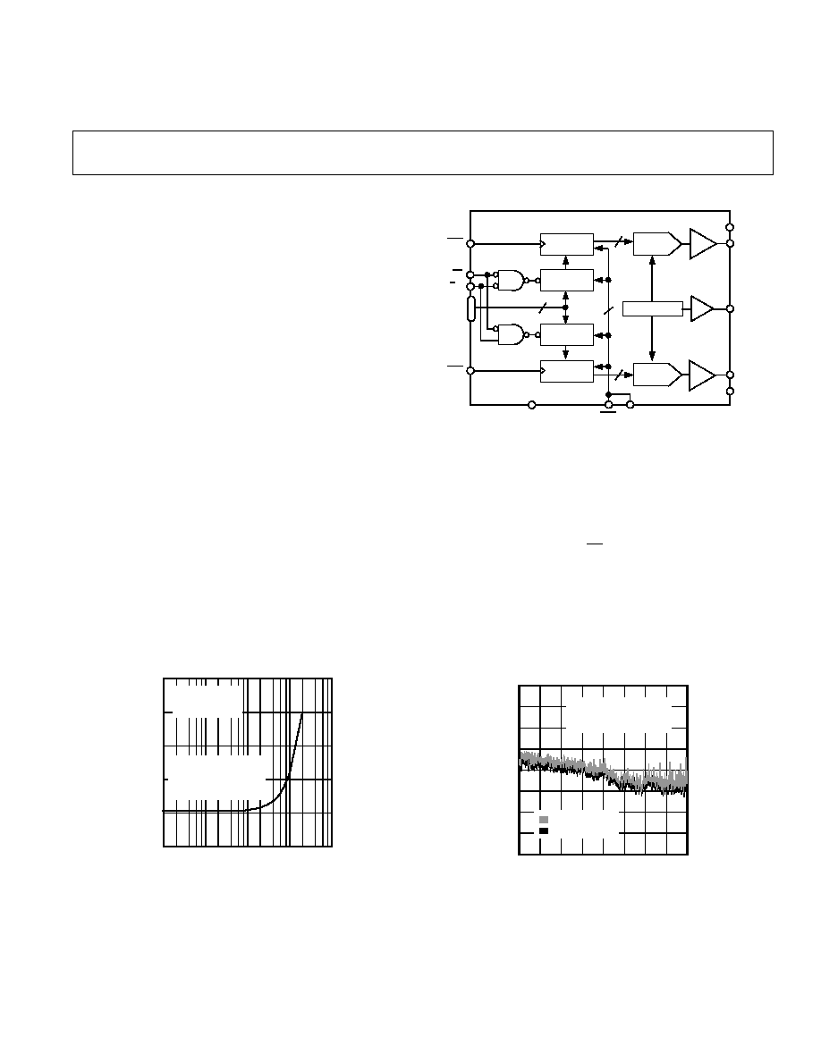
FUNCTIONAL BLOCK DIAGRAM
REV. 0
Information furnished by Analog Devices is believed to be accurate and
reliable. However, no responsibility is assumed by Analog Devices for its
use, nor for any infringements of patents or other rights of third parties
which may result from its use. No license is granted by implication or
otherwise under any patent or patent rights of Analog Devices.
The high speed parallel data interface connects to the fastest
processors without wait states. The double-buffered input struc-
ture allows the user to load the input registers one at a time,
then a single load strobe tied to both LDA + LDB inputs will
update both DAC outputs simultaneously. LDA and LDB can
also be activated independently to immediately update their re-
spective DAC registers. An address input decodes DAC A or
DAC B when the chip select CS input is strobed. An asynchro-
nous reset input sets the output to zero scale. The MSB bit can
be used to establish a preset to midscale when the reset input is
strobed.
The AD8582 is available in the 24-pin plastic DIP and the sur-
face mount SOIC-24. Each part is fully specified for operation
over –40
°C to +85°C, and the full +5 V ± 5% power supply
range.
FEATURES
Complete Dual 12-Bit DAC
No External Components
Single +5 Volt Operation
1 mV/Bit with 4.095 V Full Scale
True Voltage Output,
±5 mA Drive
Very Low Power: 5 mW
APPLICATIONS
Digitally Controlled Calibration
Portable Equipment
Servo Controls
Process Control Equipment
PC Peripherals
+5 Volt, Parallel Input
Complete Dual 12-Bit DAC
GENERAL DESCRIPTION
The AD8582 is a complete, parallel input, dual 12-bit, voltage
output DAC designed to operate from a single +5 volt supply.
Built using a CBCMOS process, this monolithic DAC offers the
user low cost, and ease-of-use in +5 volt only systems.
Included on the chip, in addition to the DACs, are a rail-to-rail
amplifier, latch and reference. The reference (VREF) is trimmed
to 2.5 volts output, and the on-chip amplifier gains up the DAC
output to 4.095 volts full scale. The user needs only supply a +5
volt supply.
The AD8582 is coded natural binary. The op amp output
swings from 0 volt to +4.095 volts for a one-millivolt-per-bit
resolution, and is capable of driving
±5 mA. Operation down to
4.3 V is possible with output load currents less than 1 mA.
DATA
REFERENCE
12-BIT
DAC A
REGISTER
INPUT A
REGISTER
12-BIT
DAC B
REGISTER
INPUT B
REGISTER
12
2
12
VDD
VOUTA
VOUTB
VREF
AGND
DGND
MSB
RST
LDA
CS
A/B
LDB
AD8582
OUTPUT LOAD CURRENT – mA
V
DD
MIN
–
Volts
5.0
4.4
4.0
0.01
0.1
100
10
1.0
4.2
4.6
4.8
VFS
≤ 1 LSB
DATA = FFFH
TA = +25°C
PROPER OPERATION
WHEN VDD SUPPLY
VOLTAGE ABOVE
CURVE
Figure 1. Minimum Supply Voltage vs. Load
2.0
–2.0
4096
–1.0
–1.5
0
0.0
–0.5
0.5
1.0
1.5
3072
2048
1024
DIGITAL INPUT CODE – Decimal
LINEARITY
ERROR
–
LSB
V
DD
= +5V
T
A
= –55°C, +25°C, +85°C
= +25°C & +85°C
= –55°C
Figure 2. Linearity Error vs. Digital Code and Temperature
相關PDF資料 |
PDF描述 |
|---|---|
| VI-B1B-MV-F1 | CONVERTER MOD DC/DC 95V 150W |
| VI-J2T-MZ-S | CONVERTER MOD DC/DC 6.5V 25W |
| VI-J3R-MZ-S | CONVERTER MOD DC/DC 7.5V 25W |
| VI-B14-MV-F4 | CONVERTER MOD DC/DC 48V 150W |
| D38999/24KC98PB | CONN RCPT 10POS JAM NUT W/PINS |
相關代理商/技術參數 |
參數描述 |
|---|---|
| AD8582AR | 功能描述:IC DAC 12BIT DUAL 5V 24-SOIC RoHS:否 類別:集成電路 (IC) >> 數據采集 - 數模轉換器 系列:- 產品培訓模塊:Data Converter Fundamentals DAC Architectures 標準包裝:750 系列:- 設置時間:7µs 位數:16 數據接口:并聯 轉換器數目:1 電壓電源:雙 ± 功率耗散(最大):100mW 工作溫度:0°C ~ 70°C 安裝類型:表面貼裝 封裝/外殼:28-LCC(J 形引線) 供應商設備封裝:28-PLCC(11.51x11.51) 包裝:帶卷 (TR) 輸出數目和類型:1 電壓,單極;1 電壓,雙極 采樣率(每秒):143k |
| AD8582AR-REEL | 功能描述:IC DAC DUAL 12BIT 5V 24SOIC RoHS:否 類別:集成電路 (IC) >> 數據采集 - 數模轉換器 系列:- 產品培訓模塊:Data Converter Fundamentals DAC Architectures 標準包裝:750 系列:- 設置時間:7µs 位數:16 數據接口:并聯 轉換器數目:1 電壓電源:雙 ± 功率耗散(最大):100mW 工作溫度:0°C ~ 70°C 安裝類型:表面貼裝 封裝/外殼:28-LCC(J 形引線) 供應商設備封裝:28-PLCC(11.51x11.51) 包裝:帶卷 (TR) 輸出數目和類型:1 電壓,單極;1 電壓,雙極 采樣率(每秒):143k |
| AD8582ARZ | 功能描述:IC DAC 12BIT DUAL 5V 24-SOIC RoHS:是 類別:集成電路 (IC) >> 數據采集 - 數模轉換器 系列:- 產品培訓模塊:Lead (SnPb) Finish for COTS Obsolescence Mitigation Program 標準包裝:50 系列:- 設置時間:4µs 位數:12 數據接口:串行 轉換器數目:2 電壓電源:單電源 功率耗散(最大):- 工作溫度:-40°C ~ 85°C 安裝類型:表面貼裝 封裝/外殼:8-TSSOP,8-MSOP(0.118",3.00mm 寬) 供應商設備封裝:8-uMAX 包裝:管件 輸出數目和類型:2 電壓,單極 采樣率(每秒):* 產品目錄頁面:1398 (CN2011-ZH PDF) |
| AD8582ARZ-REEL | 功能描述:IC DAC DUAL 12BIT 5V 24SOIC RoHS:是 類別:集成電路 (IC) >> 數據采集 - 數模轉換器 系列:- 產品培訓模塊:Data Converter Fundamentals DAC Architectures 標準包裝:750 系列:- 設置時間:7µs 位數:16 數據接口:并聯 轉換器數目:1 電壓電源:雙 ± 功率耗散(最大):100mW 工作溫度:0°C ~ 70°C 安裝類型:表面貼裝 封裝/外殼:28-LCC(J 形引線) 供應商設備封裝:28-PLCC(11.51x11.51) 包裝:帶卷 (TR) 輸出數目和類型:1 電壓,單極;1 電壓,雙極 采樣率(每秒):143k |
| AD8582CHIPS | 制造商:AD 制造商全稱:Analog Devices 功能描述:+5 Volt, Parallel Input Complete Dual 12-Bit DAC |
發布緊急采購,3分鐘左右您將得到回復。