- 您現(xiàn)在的位置:買賣IC網(wǎng) > PDF目錄373950 > AD8594AR (ANALOG DEVICES INC) CMOS Single Supply Rail-to-Rail Input/Output Operational Amplifiers with Shutdown PDF資料下載
參數(shù)資料
| 型號: | AD8594AR |
| 廠商: | ANALOG DEVICES INC |
| 元件分類: | 運(yùn)動控制電子 |
| 英文描述: | CMOS Single Supply Rail-to-Rail Input/Output Operational Amplifiers with Shutdown |
| 中文描述: | QUAD OP-AMP, 30000 uV OFFSET-MAX, 2.2 MHz BAND WIDTH, PDSO16 |
| 封裝: | SOIC-16 |
| 文件頁數(shù): | 11/15頁 |
| 文件大小: | 227K |
| 代理商: | AD8594AR |
AD8591/AD8592/AD8594
–11–
REV. A
The U1-A amplifier is configured as a unity gain buffer driving a
1 nF capacitor. The input signal is connected to the noninverting
input, while the sample clock controls the shutdown for that
amplifier. When the sample clock is high, the U1-A amplifier is
active and the output follows V
IN
. Once the sample clock goes
low, U1-A shuts down with the output of the amplifier going to
a high impedance state, holding the voltage on the C1 capacitor.
The U1-B amplifier is used as a unity gain buffer to prevent load-
ing on C1. Because of the low input bias current of the U1-B
CMOS input stage and the high impedance state of the U1-A
output in shutdown, there is very little voltage droop from C1
during the Hold period. This circuit can be used with sample
frequencies as high as 500kHz and as low as below 1Hz. Even
lower voltage droop can be achieved for very low sample rates
by increasing the value of C1.
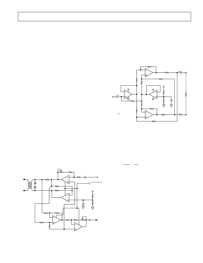
Direct Access Arrangement for PCMCIA Modems
(Telephone Line Interface)
Figure 38 illustrates a +5V transmit/receive telephone line
interface for 600
systems. It allows full duplex transmission of
signals on a transformer-coupled 600
line in a differential
manner. Amplifier A1 provides gain that can be adjusted to
meet the modem output drive requirements. Both A1 and A2
are configured to apply the largest possible signal on a single
supply to the transformer. Because of the AD8594’s high output
current drive and low dropout voltages, the largest signal avail-
able on a single +5V supply is approximately 4.5Vp-p into a
600
transmission system. Amplifier A3 is configured as a
difference amplifier for two reasons: (1)It prevents the transmit
signal from interfering with the receive signal and (2)it extracts
the receive signal from the transmission line for amplification by
A4. Amplifier A4’s gain can be adjusted in the same manner as
A1’s to meet the modem’s input signal requirements. Standard
resistor values permit the use of SIP (Single In-line Package)
format resistor arrays. Couple this with the AD8594 16-lead
TSSOP or SOIC footprint, and this circuit offers a compact,
cost effective solution.
R7
10k
V
R8
10k
V
+5V
6.2V
6.2V
TRANSMIT
TxA
RECEIVE
RxA
C1
0.1
m
F
R1
10k
V
R2
9.09k
V
2k
V
P1
Tx GAIN
ADJUST
A1
A2
A3
A4
A1, A2 = 1/2 AD8592
A3, A4 = 1/2 AD8592
R3
360
V
1:1
T1
TO TELEPHONE
LINE
1
2
3
9
8
7
2
3
1
8
7
9
10
m
F
R5
10k
V
R6
10k
V
R9
10k
V
R14
14.3k
V
R10
10k
V
R11
10k
V
R12
10k
V
R13
10k
V
C2
0.1
m
F
P2
Rx GAIN
ADJUST
2k
V
Z
O
600
V
MIDCOM
671-8005
SHUTDOWN
6
5
6
5
Figure 38. A Single Supply Direct Access Arrangement for
PCMCIA Modems
Single Supply Differential Line Driver
Figure 39 shows a single supply differential line driver circuit that
can drive a 600
load with less than 0.7% distortion from 20 Hz
to 15 kHz with an input signal of 4 V p-p and a single +5 V supply.
The design uses an AD8594 to mimic the performance of a fully
balanced transformer based solution. However, this design occu-
pies much less board space while maintaining low distortion and
can operate down to dc. Like the transformer based design, either
output can be shorted to ground for unbalanced line driver applica-
tions without changing the circuit gain of 1.
R3
10k
V
R
L
600
V
C1
22
m
F
A2
9
8
7
3
1
2
A1
+5V
R1
10k
V
R2
10k
V
R11
10k
V
R7
10k
V
8
7
7
A1
+5V
+5V
R8
100k
V
R9
100k
V
C2
1
m
F
R12
10k
V
R14
50
V
A2
1
2
3
R6
10k
V
R13
10k
V
C3
47
m
F
V
O1
V
O2
C4
47
m
F
A1, A2 = 1/2 AD8592
GAIN =R2
SET: R7, R10, R11 = R2
SET: R6, R12, R13 = R3
V
IN
R10
10k
V
R5
50
V
10
4
10
4
9
Figure 39. A Low Noise, Single Supply Differential
Line Driver
R8 and R9 set up the common-mode output voltage equal to
half of the supply voltage. C1 is used to couple the input signal
and can be omitted if the input’s dc voltage is equal to half of
the supply voltage.
The circuit can also be configured to provide additional gain if
desired. The gain of the circuit is:
A
V
V
R
R
V
OUT
IN
=
=
3
2
(7)
Where:
V
OUT
= V
O1
–V
O2
,
R2
= R7 = R10 = R11 and,
R3
= R6 = R12 = R13
相關(guān)PDF資料 |
PDF描述 |
|---|---|
| AD8594ARU | CMOS Single Supply Rail-to-Rail Input/Output Operational Amplifiers with Shutdown |
| AD8599 | Dual Ultralow Distortion, Ultralow Noise Op Amp |
| AD8599ARZ | Dual Ultralow Distortion, Ultralow Noise Op Amp |
| AD8599ARZ-REEL | Dual Ultralow Distortion, Ultralow Noise Op Amp |
| AD8599ARZ-REEL7 | Dual Ultralow Distortion, Ultralow Noise Op Amp |
相關(guān)代理商/技術(shù)參數(shù) |
參數(shù)描述 |
|---|---|
| AD8594AR-REEL | 制造商:Analog Devices 功能描述:OP Amp Quad GP R-R I/O 6V 16-Pin SOIC N T/R 制造商:Rochester Electronics LLC 功能描述:QUAD, CMOS RAIL-RAIL OP AMP W/SHUTDOWN - Tape and Reel |
| AD8594AR-REEL7 | 制造商:Analog Devices 功能描述:OP Amp Quad GP R-R I/O 6V 16-Pin SOIC N T/R |
| AD8594ARU | 制造商:AD 制造商全稱:Analog Devices 功能描述:CMOS Single Supply Rail-to-Rail Input/Output Operational Amplifiers with Shutdown |
| AD8594ARU-REEL | 制造商:Analog Devices 功能描述:OP Amp Quad GP R-R I/O 6V 16-Pin TSSOP T/R 制造商:Rochester Electronics LLC 功能描述:QUAD, CMOS RAIL-RAIL OP AMP W/SHUTDOWN - Tape and Reel |
| AD8594ARUZ-REEL | 功能描述:IC OPAMP GP R-R CMOS 16TSSOP RoHS:是 類別:集成電路 (IC) >> Linear - Amplifiers - Instrumentation 系列:- 標(biāo)準(zhǔn)包裝:2,500 系列:- 放大器類型:通用 電路數(shù):1 輸出類型:滿擺幅 轉(zhuǎn)換速率:0.11 V/µs 增益帶寬積:350kHz -3db帶寬:- 電流 - 輸入偏壓:4nA 電壓 - 輸入偏移:20µV 電流 - 電源:260µA 電流 - 輸出 / 通道:20mA 電壓 - 電源,單路/雙路(±):2.7 V ~ 36 V,±1.35 V ~ 18 V 工作溫度:-40°C ~ 85°C 安裝類型:表面貼裝 封裝/外殼:8-SOIC(0.154",3.90mm 寬) 供應(yīng)商設(shè)備封裝:8-SO 包裝:帶卷 (TR) |
發(fā)布緊急采購,3分鐘左右您將得到回復(fù)。