- 您現在的位置:買賣IC網 > PDF目錄373950 > AD8600 (Analog Devices, Inc.) 16-Channel, 8-Bit Multiplying DAC PDF資料下載
參數資料
| 型號: | AD8600 |
| 廠商: | Analog Devices, Inc. |
| 英文描述: | 16-Channel, 8-Bit Multiplying DAC |
| 中文描述: | 16通道,8位乘法DAC |
| 文件頁數: | 9/16頁 |
| 文件大小: | 236K |
| 代理商: | AD8600 |
AD8600
REV. 0
–9–
Power Supply and Grounding Considerations
T he low power consumption of the AD8600 is a direct result of
circuit design optimizing using a CBCMOS process. T he over-
all power dissipation of 120 mW translates to a total supply cur-
rent of only 24 mA for 16 DACs. T hus, each DAC consumes
only 1.5 mA. Because the digital interface is comprised entirely
of CMOS logic, the power dissipation is dependent upon the
logic input levels. As expected for CMOS, the lowest power
dissipation is achieved when the input level is either close to
ground or +5 V. T hus, to minimize the power consumption,
CMOS logic should be used to interface to the AD8600.
T he AD8600 has multiple supply pins. V
CC
(Pins 4 and 42) is
the output amplifiers’ positive supply, and V
EE
(Pins 5 and 41)
the amplifiers’ negative supply. T he digital input circuitry is
powered by V
DD1
(Pin 14), and finally the DAC register and R-
2R ladder switches are powered by V
DD2
(Pin 44). T o minimize
noise feedthrough from the supplies, each supply pin should be
decoupled with a 0.1
μ
F ceramic capacitor close to the pin.
When applying power to the device, it is important for the digi-
tal supply, V
DD2
, to power on before the reference voltage and
for V
REF
to remain less than 0.3 V above V
DD2
during normal
operation. Otherwise, an inherent diode will energize, and it
could damage the AD8600.
In order to improve ESD resistance, the AD8600 has several
ESD protection diodes on its various pins. T hese diodes shunt
ESD energy to the power supplies and protect the sensitive ac-
tive circuitry. During normal operation, all the ESD diodes are
reversed biased and do not affect the part. However, if overvolt-
ages occur on the various inputs, these diodes will energize. If
the overvoltage is due to ESD, the electrical spike is typically
short enough so that the part is not damaged. However, if the
overvoltage is continuous and has sufficient current, the part
could be damaged. T o protect the part, it is important not to
forward bias any of the ESD protection diodes during normal
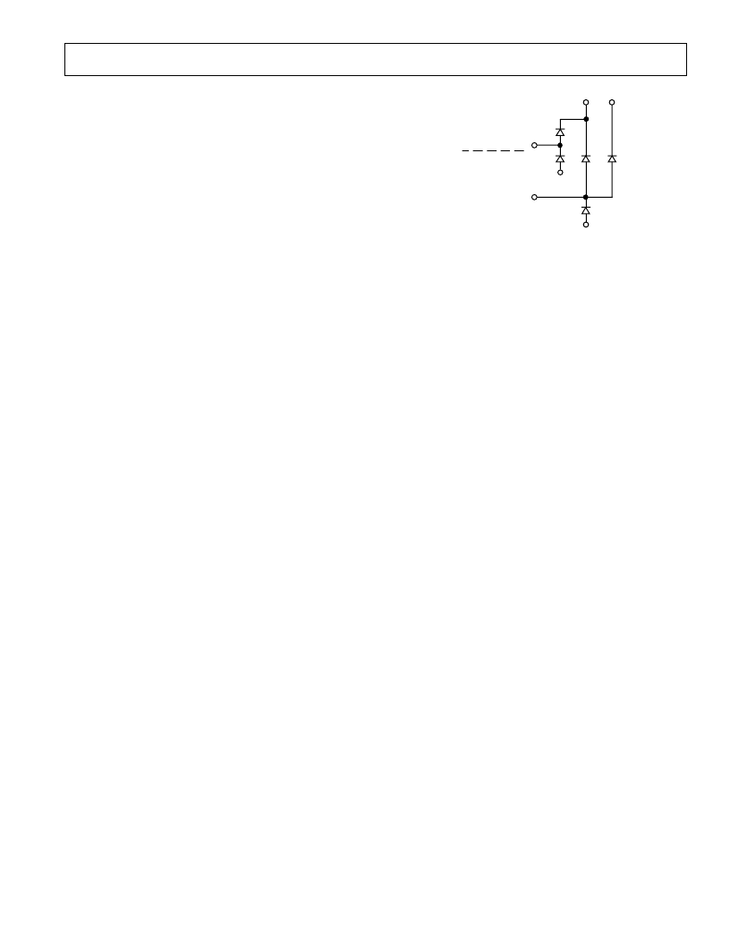
operation or during power up. Figure 18 shows the location of
these diodes. For example, the digital inputs have diodes con-
nected to V
CC
and from DGND1. T hus, the voltage on any
digital input should never exceed the analog supply or drop be-
low ground, which is also indicated in the absolute maximum
ratings.
DGND1
V
CC
V
DD2
DACGND
V
REF
ALL DIGITAL INPUTS
(A0–A3, DB0–DB7)
(R/
W
,
CS
,
EN
,
LD
,
RS
)
Figure 18. ESD Protection Diode Locations
Attention should be paid to the ground pins of the AD8600 to
ensure that noise is not introduced to the output. T he pin la-
beled DACGND (Pin 3) is actually the ground for the R-2R
ladder, and because of this, it is important to connect this pin to
a high quality analog ground. Ideally, the analog ground should
be an actual ground plane. T his helps create a low impedance,
low noise ground to maintain accuracy in the analog circuitry.
T he digital ground pins (DGND1 at Pin 32 and DGND2 at
Pin 43) provide the ground reference for the internal digital cir-
cuitry and latches. T he first thought may be to connect both of
these pins to the system digital ground. However, this is not the
best choice because of the high noise typically found on a
system’s digital ground. T his noise can feed through to the out-
put through the DAC’s ground pins. Instead, DGND1 and
DGND2 should be connected to the analog ground plane. T he
actual switching current in these pins is small and should not
degrade the analog ground.
5 V Output Swing
T he output swing is limited to 1.0 V below the positive supply.
T his gives a maximum output of +4.0 V on a +5 V supply. T o
increase the output range, the analog supply, V
CC
, and the DAC
ladder supply, V
DD2
, can be increased to +7 V. T his allows an
output of +5 V with a 5 V reference. V
DD1
should remain at
+5 V to ensure that the input logic levels do not change.
Reference Input Considerations
T he AD8600 is designed for one reference to drive all 16 DACs.
T he reference pin (V
REF
) is connected directly to the R-2R lad-
ders of each DAC. With 16 DACs in parallel, the input imped-
ance is typically 2 k
and a minimum of 1.2 k
. T he input
resistance is code dependent. T hus, the chosen reference device
must be able to drive this load. Some examples of +2.5 V refer-
ences that easily interface to the AD8600 are the REF43,
AD680, and AD780. T he unique architecture ensures that the
reference does not have to supply “shoot through” current,
which is a condition in some voltage mode DACs where the ref-
erence is momentarily connected to ground through the CMOS
switches. By eliminating this possibility, all 16 DACs in the
AD8600 can easily be driven from a single reference.
相關PDF資料 |
PDF描述 |
|---|---|
| AD8600AP | 16-Channel, 8-Bit Multiplying DAC |
| AD8600CHIPS | 16-Channel, 8-Bit Multiplying DAC |
| AD8601ART | Precision CMOS Single Supply Rail-to-Rail Input/Output Wideband Operational Amplifiers |
| AD8601DRT | Precision CMOS Single Supply Rail-to-Rail Input/Output Wideband Operational Amplifiers |
| AD8602 | Precision CMOS Single Supply Rail-to-Rail Input/Output Wideband Operational Amplifiers |
相關代理商/技術參數 |
參數描述 |
|---|---|
| AD8600AP | 制造商:Analog Devices 功能描述:DAC 16-CH R-2R 8-bit 44-Pin PLCC 制造商:Rochester Electronics LLC 功能描述:16 CHANNEL 8-BIT MULT.DAC - Bulk 制造商:Analog Devices 功能描述:Digital-Analog Converter IC Interface Ty |
| AD8600AP-REEL | 制造商:Analog Devices 功能描述:DAC 16-CH R-2R 8-bit 44-Pin PLCC T/R 制造商:Rochester Electronics LLC 功能描述:16 CHANNEL 8-BIT MULT.DAC - Tape and Reel |
| AD8600APZ | 功能描述:IC DAC MULT 16CH 8BIT 44PLCC RoHS:是 類別:集成電路 (IC) >> 數據采集 - 數模轉換器 系列:- 標準包裝:1 系列:- 設置時間:4.5µs 位數:12 數據接口:串行,SPI? 轉換器數目:1 電壓電源:單電源 功率耗散(最大):- 工作溫度:-40°C ~ 125°C 安裝類型:表面貼裝 封裝/外殼:8-SOIC(0.154",3.90mm 寬) 供應商設備封裝:8-SOICN 包裝:剪切帶 (CT) 輸出數目和類型:1 電壓,單極;1 電壓,雙極 采樣率(每秒):* 其它名稱:MCP4921T-E/SNCTMCP4921T-E/SNRCTMCP4921T-E/SNRCT-ND |
| AD8600APZ-REEL | 功能描述:IC DAC MULT 16CH 8BIT 44PLCC RoHS:是 類別:集成電路 (IC) >> 數據采集 - 數模轉換器 系列:- 產品培訓模塊:Lead (SnPb) Finish for COTS Obsolescence Mitigation Program 標準包裝:1,000 系列:- 設置時間:1µs 位數:8 數據接口:串行 轉換器數目:8 電壓電源:雙 ± 功率耗散(最大):941mW 工作溫度:0°C ~ 70°C 安裝類型:表面貼裝 封裝/外殼:24-SOIC(0.295",7.50mm 寬) 供應商設備封裝:24-SOIC W 包裝:帶卷 (TR) 輸出數目和類型:8 電壓,單極 采樣率(每秒):* |
發布緊急采購,3分鐘左右您將得到回復。