- 您現在的位置:買賣IC網 > PDF目錄373951 > AD8608AR (ANALOG DEVICES INC) Precision Low noise CMOS Rail-to-Rail Input/Output Operational Amplifiers PDF資料下載
參數資料
| 型號: | AD8608AR |
| 廠商: | ANALOG DEVICES INC |
| 元件分類: | 運動控制電子 |
| 英文描述: | Precision Low noise CMOS Rail-to-Rail Input/Output Operational Amplifiers |
| 中文描述: | QUAD OP-AMP, 750 uV OFFSET-MAX, 10 MHz BAND WIDTH, PDSO14 |
| 封裝: | MS-012AB, SOIC-14 |
| 文件頁數: | 17/20頁 |
| 文件大小: | 559K |
| 代理商: | AD8608AR |
AD8605/AD8606/AD8608
INSTRUMENTATION AMPLIFIERS
The low offset voltage and low noise of the AD8605 make it a
great amplifier for instrumentation applications.
Rev. D | Page 17 of 20
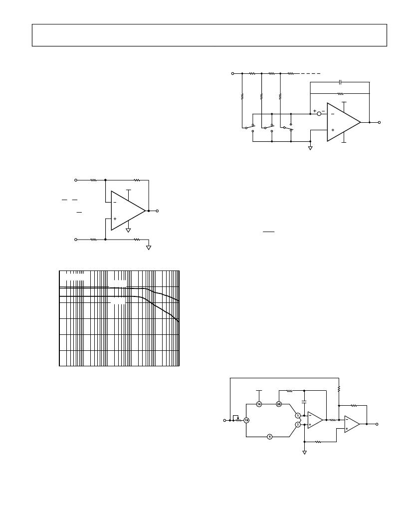
Difference amplifiers are widely used in high accuracy circuits
to improve the common-mode rejection ratio.
Figure 53 shows a simple difference amplifier. The CMRR of the
circuit is plotted versus frequency. Figure 54 shows the
common-mode rejection for a unity gain configuration and for
a gain of 10.
Making (R4/R3) = (R2/R1) and choosing 0.01% tolerance yields
a CMRR of 74 dB and minimizes the gain error at the output.
AD8605
5V
V2
V1
R1
1k
R3
1k
R2
10k
R4
10k
V
OUT
R
4
R
3
R
2
R
1
=
V
OUT
= R
V
2 –
V
1)
1
R
2
0
Figure 53. Difference Amplifier, A
V
= 10
FREQUENCY (Hz)
120
100
0
100
10M
1k
C
10k
100k
1M
60
40
20
80
A
V
= 10
V
SY
= ±2.5V
A
V
= 1
0
Figure 54. Difference Amplifier CMRR vs. Frequency
D/A CONVERSION
The low input bias current and offset voltage of the AD8605
make it an excellent choice for buffering the output of a current
output DAC.
Figure 55 shows a typical implementation of the AD8605 at the
output of a 12-bit DAC.
The DAC8143 output current is converted to a voltage by the
feedback resistor. The equivalent resistance at the output of the
DAC varies with the input code, as does the output capacitance.
R2
AD8605
V
OS
R
F
C
F
R2
R2
V+
V–
0
R
R
R
V
REF
Figure 55. Simplified Circuit of the DAC8143 with AD8605 Output Buffer
To optimize the performance of the DAC, insert a capacitor in
the feedback loop of the AD8605 to compensate the amplifier
from the pole introduced by the output capacitance of the DAC.
Typical values for C
F
are in the range of 10 pF to 30 pF; it can be
adjusted for the best frequency response. The total error at the
output of the op amp can be computed by the formula:
+
=
q
R
Re
V
E
F
OS
O
1
where
Req
is the equivalent resistance seen at the output of the
DAC. As mentioned above,
Req
is code dependant and varies
with the input. A typical value for
Req
is 15 k. Choosing a
feedback resistor of 10 k yields an error of less than 200 μV.
Figure 56 shows the implementation of a dual-stage buffer at
the output of a DAC. The first stage is used as a buffer.
Capacitor C1, with Req, creates a low-pass filter and thus
provides phase lead to compensate for frequency response. The
second stage of the AD8606 is used to provide voltage gain at
the output of the buffer.
Grounding the positive input terminals in both stages reduces
errors due to the common-mode output voltage. Choosing R1,
R2, and R3 to match within 0.01% yields a CMRR of 74 dB and
maintains minimum gain error in the circuit.
R
FB
V
DD
DB11
OUT1
AD7545
AGND
R
CS
R
P
V
IN
15V
V
OUT
V
REF
1/2
AD8606
1/2
AD8606
R4
5k
10%
R1
10k
R2
10k
R3
20k
C1
33pF
0
Figure 56. Bipolar Operation
相關PDF資料 |
PDF描述 |
|---|---|
| AD8608ARU | Precision Low noise CMOS Rail-to-Rail Input/Output Operational Amplifiers |
| AD8605ART-REEL | Precision Low noise CMOS Rail-to-Rail Input/Output Operational Amplifiers |
| AD8605ART-REEL7 | Precision Low noise CMOS Rail-to-Rail Input/Output Operational Amplifiers |
| AD8605ARTZ-REEL | Precision Low noise CMOS Rail-to-Rail Input/Output Operational Amplifiers |
| AD8605ARTZ-REEL7 | Precision Low noise CMOS Rail-to-Rail Input/Output Operational Amplifiers |
相關代理商/技術參數 |
參數描述 |
|---|---|
| AD8608ARN | 制造商:未知廠家 制造商全稱:未知廠家 功能描述:Operational Amplifier |
| AD8608AR-REEL | 制造商:Analog Devices 功能描述:OP Amp Quad GP R-R I/O 5.5V 14-Pin SOIC N T/R |
| AD8608AR-REEL7 | 制造商:Analog Devices 功能描述:OP Amp Quad GP R-R I/O 5.5V 14-Pin SOIC N T/R |
| AD8608ARU | 制造商:Analog Devices 功能描述:IC OP-AMP QUAD R/R |
| AD8608ARU-REEL | 制造商:Analog Devices 功能描述:OP Amp Quad GP R-R I/O 5.5V 14-Pin TSSOP T/R |
發布緊急采購,3分鐘左右您將得到回復。