- 您現在的位置:買賣IC網 > PDF目錄373952 > AD8612ARU (ANALOG DEVICES INC) Ultrafast 4 ns Single Supply Comparators PDF資料下載
參數資料
| 型號: | AD8612ARU |
| 廠商: | ANALOG DEVICES INC |
| 元件分類: | 運動控制電子 |
| 英文描述: | Ultrafast 4 ns Single Supply Comparators |
| 中文描述: | COMPARATOR, 7000 uV OFFSET-MAX, 4.5 ns RESPONSE TIME, PDSO14 |
| 封裝: | TSSOP-14 |
| 文件頁數: | 8/12頁 |
| 文件大小: | 130K |
| 代理商: | AD8612ARU |
AD8611/AD8612
–8–
REV. 0
The AD8611 is stable with all values of capacitive load; however,
loading an output with greater than 30 pF will increase the propa-
gation delay of that channel. Capacitive loads greater than 500 pF
will also create some ringing on the output wave. Table II shows
propagation delay versus several values of load capacitance. The
loading on one output of the AD8611 does not affect the propaga-
tion delay of the other output.
Table II. Propagation Delay vs. Capacitive Load
Using the Latch to Maintain a Constant Output
The latch input to the AD8611/AD8612 can be used to retain
data at the output of the comparator. When the latch voltage goes
high, the output voltage will remain in its previous state, indepen-
dent of changes in the input voltage.
The setup time for the AD8611/AD8612 is 0.5 ns and the hold
time is 0.5 ns. Setup time is defined as the minimum amount of
time the input voltage must remain in a valid state before the
latch is activated for the latch to function properly. Hold time is
defined as the amount of time the input must remain constant
after the latch voltage goes high for the output to remain latched
its voltage.
The latch input is TTL and CMOS compatible, so a logic high is
a minimum of 2.0 V and a logic low is a maximum of 0.8 V. The
latch circuitry in the AD8611/AD8612 has no built-in hysteresis.
Input Stage and Bias Currents
The AD8611 and AD8612 use a bipolar PNP differential input
stage. This enables the input common-mode voltage range to extend
from within 2.0 V of the positive supply voltage to 200 mV below the
negative supply voltage. Therefore, using a single 5 V supply, the
input common-mode voltage range is –200 mV to +3.0 V. Input
common-mode voltage is the average of the voltages at the two
inputs. For proper operation, the input common-mode voltage
should be kept within the common-mode voltage range.
The input bias current for the AD8611/AD8612 is 4
μ
A, which
is the amount of current that flows from each input of the com-
parator. This bias current will go to zero on an input that is high
and will double on an input that is low, which is a characteristic
common to any bipolar comparator. Care should be taken in
choosing resistances to be connected around the comparator as
large resistors could cause significant voltage drops due to the
input bias current.
The input capacitance for the AD8611/AD8612 is typically 3 pF.
This is measured by inserting a 5 k
source resistance in series
with the input and measuring the change in propagation delay.
Using Hysteresis
Hysteresis can easily be added to a comparator through the addi-
tion of positive feedback. Adding hysteresis to a comparator offers
an advantage in noisy environments where it is not desirable for
the output to toggle between states when the input signal is close
to the switching threshold. Figure 18 shows a simple method for
configuring the AD8611 or AD8612 with hysteresis.
V
REF
R1
SIGNAL
COMPARATOR
R2
C
F
Figure 18. Configuring the AD8611/AD8612 with
Hysteresis
Here, the input signal is connected directly to the inverting input
of the comparator. The output is fed back to the noninverting
input through R1 and R2. The ratio of R1 to R1 + R2 establishes
the width of the hysteresis window with V
REF
setting the center of
the window, or the average switching voltage. The Q output will
switch low when the input voltage is greater than V
HI
, and will
not switch high again until the input voltage is less than V
LO
as
given in Equation 1:
V
V
V
R
+
R
R
V
HI
REF
REF
=
(
)
+
+
1 5
.
1
1
2
(1)
V
V
R
+
1
R
R
LO
REF
=
×
2
2
Where
V
+
is the positive supply voltage.
The capacitor C
F
is optional and can be added to introduce a
pole into the feedback network. This has the effect of increasing
the amount of hysteresis at high frequencies, which is useful when
comparing relatively slow signals in high-frequency noise envi-
ronments. At frequencies greater than f
P
, the hysteresis window
approaches V
HI
= V
+
– 1.5 V and V
LO
= 0 V. For frequencies less
than
P
, the threshold voltages remain as in Equation 1.
Clock Timing Recovery
Comparators are often used in digital systems to recover clock
timing signals. High-speed square waves transmitted over a distance,
even tens of centimeters, can become distorted due to stray capaci-
tance and inductance. Poor layout or improper termination can also
cause reflections on the transmission line, further distorting the
signal waveform. A high-speed comparator can be used to recover
the distorted waveform while maintaining a minimum of delay.
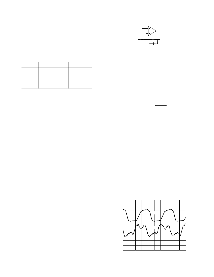
Figure 19 shows the AD8611 used to recover a 65 MHz, 100 mV
peak-to-peak distorted clock signal into a 4 V peak-to-peak square
wave. The lower trace is the input to the AD8611 and the upper
trace is the Q output from the comparator. The AD8611 is powered
from a 5 V single supply.
TIME
–
10ns/DIV
2V/DIV
V
OUT
V
IN
20mV/DIV
Figure 19. Using the AD8611 to Recover a Noisy Clock Signal
C
L
< 10 pF
33 pF
100 pF
390 pF
680 pF
PD
Rising
3.5 ns
5 ns
8 ns
14.5 ns
26 ns
PD
Falling
3.5 ns
5 ns
7 ns
10 ns
15 ns
相關PDF資料 |
PDF描述 |
|---|---|
| AD8614 | Single and Quad +18 V Operational Amplifiers |
| AD8614ART | Single and Quad +18 V Operational Amplifiers |
| AD8644 | Single and Quad +18 V Operational Amplifiers |
| AD8644AR2 | Single and Quad +18 V Operational Amplifiers |
| AD8644ARU | Single and Quad +18 V Operational Amplifiers |
相關代理商/技術參數 |
參數描述 |
|---|---|
| AD8612ARU-REEL | 功能描述:IC COMP DUAL 4NS FAST 14-TSSOP RoHS:否 類別:集成電路 (IC) >> 線性 - 比較器 系列:- 產品培訓模塊:Lead (SnPb) Finish for COTS Obsolescence Mitigation Program 標準包裝:2,500 系列:- 類型:通用 元件數:1 輸出類型:CMOS,推挽式,滿擺幅,TTL 電壓 - 電源,單路/雙路(±):2.5 V ~ 5.5 V,±1.25 V ~ 2.75 V 電壓 - 輸入偏移(最小值):5mV @ 5.5V 電流 - 輸入偏壓(最小值):1pA @ 5.5V 電流 - 輸出(標準):- 電流 - 靜態(最大值):24µA CMRR, PSRR(標準):80dB CMRR,80dB PSRR 傳輸延遲(最大):450ns 磁滯:±3mV 工作溫度:-40°C ~ 85°C 封裝/外殼:6-WFBGA,CSPBGA 安裝類型:表面貼裝 包裝:管件 其它名稱:Q3554586 |
| AD8612ARUZ | 功能描述:IC COMP DUAL 4NS FAST 14-TSSOP RoHS:是 類別:集成電路 (IC) >> 線性 - 比較器 系列:- 標準包裝:1 系列:- 類型:通用 元件數:1 輸出類型:CMOS,開路集電極,TTL 電壓 - 電源,單路/雙路(±):2.7 V ~ 5.5 V 電壓 - 輸入偏移(最小值):7mV @ 5V 電流 - 輸入偏壓(最小值):0.25µA @ 5V 電流 - 輸出(標準):84mA @ 5V 電流 - 靜態(最大值):120µA CMRR, PSRR(標準):- 傳輸延遲(最大):600ns 磁滯:- 工作溫度:-40°C ~ 85°C 封裝/外殼:SC-74A,SOT-753 安裝類型:表面貼裝 包裝:剪切帶 (CT) 產品目錄頁面:1268 (CN2011-ZH PDF) 其它名稱:*LMV331M5*LMV331M5/NOPBLMV331M5CT |
| AD8612ARUZ | 制造商:Analog Devices 功能描述:IC DUAL COMPARATOR |
| AD8612ARUZ-REEL | 功能描述:IC COMP DUAL 4NS FAST 14-TSSOP RoHS:是 類別:集成電路 (IC) >> 線性 - 比較器 系列:- 產品培訓模塊:Lead (SnPb) Finish for COTS Obsolescence Mitigation Program 標準包裝:2,500 系列:- 類型:通用 元件數:1 輸出類型:CMOS,推挽式,滿擺幅,TTL 電壓 - 電源,單路/雙路(±):2.5 V ~ 5.5 V,±1.25 V ~ 2.75 V 電壓 - 輸入偏移(最小值):5mV @ 5.5V 電流 - 輸入偏壓(最小值):1pA @ 5.5V 電流 - 輸出(標準):- 電流 - 靜態(最大值):24µA CMRR, PSRR(標準):80dB CMRR,80dB PSRR 傳輸延遲(最大):450ns 磁滯:±3mV 工作溫度:-40°C ~ 85°C 封裝/外殼:6-WFBGA,CSPBGA 安裝類型:表面貼裝 包裝:管件 其它名稱:Q3554586 |
| AD8613 | 制造商:AD 制造商全稱:Analog Devices 功能描述:Low Cost Micropower, Low Noise CMOS Rail-to- Rail, Input/Output Operational Amplifiers |
發布緊急采購,3分鐘左右您將得到回復。