- 您現在的位置:買賣IC網 > PDF目錄373959 > AD9211-200EB (Analog Devices, Inc.) 10-Bit, 170/200/250 MSPS 1.8 V A/D Converter PDF資料下載
參數資料
| 型號: | AD9211-200EB |
| 廠商: | Analog Devices, Inc. |
| 英文描述: | 10-Bit, 170/200/250 MSPS 1.8 V A/D Converter |
| 中文描述: | 10位,170/200/250 MSPS的1.8弗吉尼亞州/ D轉換器 |
| 文件頁數: | 16/21頁 |
| 文件大小: | 310K |
| 代理商: | AD9211-200EB |
AD9211
Preliminary Technical Data
Clock Input Considerations
Rev. PrA | Page 16 of 21
Typical high speed ADCs use both clock edges to generate a
variety of internal timing signals, and as a result may be
sensitive to clock duty cycle. Commonly, a 5% tolerance is
required on the clock duty cycle to maintain dynamic
performance
characteristics. The AD9211 contains a DCS (duty cycle
stabilizer) that retimes the non-sampling edge, providing an
internal clock signal with a nominal 50% duty cycle. This allows
a wide range of clock input duty cycles without affecting the
performance of the AD9211. Noise and distortion performance
are nearly flat for a wide range duty cycles with the DCS on.
The duty cycle stabilizer uses a delay-locked loop (DLL) to
create the non-sampling edge. As a result, any changes to the
sampling frequency require approximately TBD clock cycles to
allow the DLL to acquire and lock to the new rate.
Jitter Considerations
High speed, high resolution ADCs are sensitive to the quality of
the clock input. The degradation in SNR at a given input
frequency (f
INPUT
) due only to aperture jitter (t
J
) can be
calculated by
×
π
2
=
J
INPUT
t
f
20
log
SNR
In the equation, the rms aperture jitter represents the root-
mean square of all jitter sources, which include the clock input,
analog input signal, and ADC aperture jitter specification. IF
under-sampling applications are particularly sensitive to jitter,
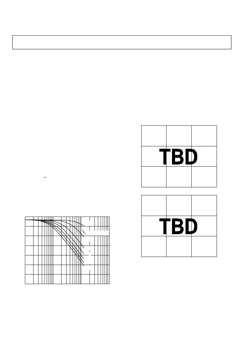
see Figure 11.
INPUT FREQUENCY (MHz)
1
40
75
70
65
60
55
50
45
1000
100
10
0.2ps
0.5ps
1.0ps
1.5ps
2.0ps
2.5ps
3.0ps
S
Figure 11. SNR vs. Input Frequency and Jitter
The clock input should be treated as an analog signal in cases
where aperture jitter may affect the dynamic range of the
AD9211. Power supplies for clock drivers should be separated
from the ADC output driver supplies to avoid modulating the
clock signal with digital noise. Low jitter, crystal-controlled
oscillators make the best clock sources. If the clock is generated
from another type of source (by gating, dividing, or other
methods), it should be retimed by the original clock at the last
step.
POWER DISSIPATION AND POWER DOWN MODE
As shown in Figure 12 and Figure 14, the power dissipated by
the AD9211 is proportional to its sample rate. The digital power
dissipation does not vary much because it is determined
primarily by the DRVDD supply and bias current of the LVDS
output drivers.
Figure 12. AD9211-170, Supply Current vs. f
SAMPLE
for f
IN
= 10.3 MHz
Figure 13. AD9211-200, Supply Current vs. f
SAMPLE
for f
IN
= 10.3 MHz
相關PDF資料 |
PDF描述 |
|---|---|
| AD9211-250EB | 10-Bit, 170/200/250 MSPS 1.8 V A/D Converter |
| AD9211BCPZ-170 | 10-Bit, 170/200/250 MSPS 1.8 V A/D Converter |
| AD9211BCPZ-200 | 10-Bit, 170/200/250 MSPS 1.8 V A/D Converter |
| AD9211BCPZ-250 | 10-Bit, 170/200/250 MSPS 1.8 V A/D Converter |
| AD9212 | Octal, 10-Bit, 40/65 MSPS Serial LVDS 1.8 V A/D Converter |
相關代理商/技術參數 |
參數描述 |
|---|---|
| AD9211-200EBZ | 功能描述:BOARD EVAL FOR AD9211-200 RoHS:是 類別:編程器,開發系統 >> 評估板 - 模數轉換器 (ADC) 系列:- 產品培訓模塊:Obsolescence Mitigation Program 標準包裝:1 系列:- ADC 的數量:1 位數:12 采樣率(每秒):94.4k 數據接口:USB 輸入范圍:±VREF/2 在以下條件下的電源(標準):- 工作溫度:-40°C ~ 85°C 已用 IC / 零件:MAX11645 已供物品:板,軟件 |
| AD9211-250EB | 制造商:AD 制造商全稱:Analog Devices 功能描述:10-Bit, 170/200/250 MSPS 1.8 V A/D Converter |
| AD9211-250EBZ | 功能描述:數據轉換 IC 開發工具 10-Bit 250 Msps ADC RoHS:否 制造商:Texas Instruments 產品:Demonstration Kits 類型:ADC 工具用于評估:ADS130E08 接口類型:SPI 工作電源電壓:- 6 V to + 6 V |
| AD9211-300EBZ | 功能描述:數據轉換 IC 開發工具 10-Bit 300 Msps ADC RoHS:否 制造商:Texas Instruments 產品:Demonstration Kits 類型:ADC 工具用于評估:ADS130E08 接口類型:SPI 工作電源電壓:- 6 V to + 6 V |
| AD9211BCPZ-170 | 制造商:AD 制造商全稱:Analog Devices 功能描述:10-Bit, 170/200/250 MSPS 1.8 V A/D Converter |
發布緊急采購,3分鐘左右您將得到回復。