- 您現(xiàn)在的位置:買賣IC網(wǎng) > PDF目錄373959 > AD9211-250EBZ (Analog Devices, Inc.) 10-Bit, 200 MSPS/250 MSPS/300 MSPS, 1.8 V Analog-to-Digital Converter PDF資料下載
參數(shù)資料
| 型號(hào): | AD9211-250EBZ |
| 廠商: | Analog Devices, Inc. |
| 英文描述: | 10-Bit, 200 MSPS/250 MSPS/300 MSPS, 1.8 V Analog-to-Digital Converter |
| 中文描述: | 10位,200 MSPS/250 MSPS/300 MSPS的,1.8 V模擬到數(shù)字轉(zhuǎn)換器 |
| 文件頁(yè)數(shù): | 22/28頁(yè) |
| 文件大小: | 1180K |
| 代理商: | AD9211-250EBZ |
第1頁(yè)第2頁(yè)第3頁(yè)第4頁(yè)第5頁(yè)第6頁(yè)第7頁(yè)第8頁(yè)第9頁(yè)第10頁(yè)第11頁(yè)第12頁(yè)第13頁(yè)第14頁(yè)第15頁(yè)第16頁(yè)第17頁(yè)第18頁(yè)第19頁(yè)第20頁(yè)第21頁(yè)當(dāng)前第22頁(yè)第23頁(yè)第24頁(yè)第25頁(yè)第26頁(yè)第27頁(yè)第28頁(yè)
AD9211
Rev. 0 | Page 22 of 28
600
–600
–400
–200
0
200
400
–3
–2
–1
0
1
2
3
E
TIME (ns)
12
10
8
6
4
2
0
–100
0
100
T
TIME (ps)
0
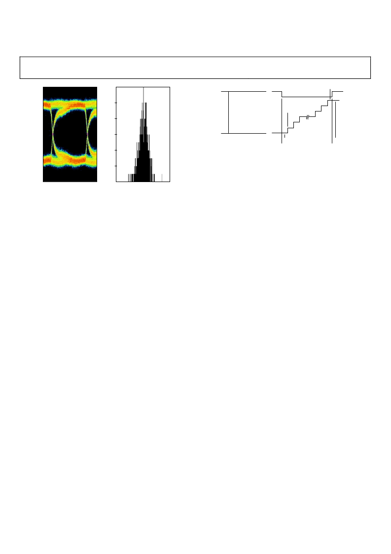
Figure 49. Data Eye for LVDS Outputs in ANSI Mode with Trace Lengths
Greater than 24 Inches on Standard FR-4, AD9211-250
The format of the output data is offset binary by default. An
example of the output coding format can be found in Table 12.
If it is desired to change the output data format to twos comple-
ment, see the AD9211 Configuration Using the SPI section.
An output clock signal is provided to assist in capturing data
from the AD9211. The DCO is used to clock the output data
and is equal to the sampling clock (CLK) rate. In single data rate
mode (SDR), data is clocked out of the AD9211 and must be
captured on the rising edge of the DCO. In double data rate
mode (DDR), data is clocked out of the AD9211 and must be
captured on the rising and falling edges of the DCO. See the
timing diagrams shown in Figure 2 and Figure 3 for more
information.
Output Data Rate and Pinout Configuration
The output data of the AD9211 can be configured to drive 10
pairs of LVDS outputs at the same rate as the input clock signal
(single data rate, or SDR, mode), or five pairs of LVDS outputs
at 2× the rate of the input clock signal (double data rate, or DDR,
mode). SDR is the default mode; the device may be reconfigured
for DDR by setting Bit 3 in Register 14 (see Table 13).
Out-of-Range (OR)
An out-of-range condition exists when the analog input voltage
is beyond the input range of the ADC. OR is a digital output
that is updated along with the data output corresponding to the
particular sampled input voltage. Thus, OR has the same
pipeline latency as the digital data. OR is low when the analog
input voltage is within the analog input range and high when
the analog input voltage exceeds the input range, as shown in
Figure 50. OR remains high until the analog input returns to
within the input range and another conversion is completed. By
logically ANDing OR with the MSB and its complement, over-
range high or underrange low conditions can be detected.
1
0
0
0
0
1
OR DATA OUTPUTS
1111
1111
1111
OR
+FS – 1 LSB
+FS – 1/2 LSB
+FS
–FS
–FS + 1/2 LSB
–FS – 1/2 LSB
0000
0000
0000
1111
1111
1111
0000
0000
0000
1111
1111
1110
0001
0000
0000
0
Figure 50. OR Relation to Input Voltage and Output Data
TIMING
The AD9211 provides latched data outputs with a pipeline delay
of seven clock cycles. Data outputs are available one propagation
delay (t
PD
) after the rising edge of the clock signal.
The length of the output data lines and loads placed on them
should be minimized to reduce transients within the AD9211.
These transients can degrade the converter’s dynamic performance.
The AD9211 also provides data clock output (DCO) intended for
capturing the data in an external register. The data outputs are valid
on the rising edge of DCO.
The lowest typical conversion rate of the AD9211 is 40 MSPS. At
clock rates below 1 MSPS, the AD9211 assumes the standby mode.
RBIAS
The AD9211 requires the user to place a 10 kΩ resistor between
the RBIAS pin and ground. This resister should have a 1%
tolerance and is used to set the master current reference of the
ADC core.
AD9211 CONFIGURATION USING THE SPI
The AD9211 SPI allows the user to configure the converter for
specific functions or operations through a structured register
space inside the ADC. This gives the user added flexibility to
customize device operation depending on the application.
Addresses are accessed (programmed or readback) serially in
one-byte words. Each byte may be further divided down into
fields, which are documented in the Memory Map section.
There are three pins that define the serial port interface or SPI
to this particular ADC. They are the SPI SCLK/DFS, SPI
SDIO/DCS, and CSB pins. The SCLK/DFS (serial clock) is used
to synchronize the read and write data presented the ADC. The
SDIO/DCS (serial data input/output) is a dual-purpose pin that
allows data to be sent and read from the internal ADC memory
map registers. The CSB is an active low control that enables or
disables the read and write cycles (see Table 9).
相關(guān)PDF資料 |
PDF描述 |
|---|---|
| AD9211-300EBZ | 10-Bit, 200 MSPS/250 MSPS/300 MSPS, 1.8 V Analog-to-Digital Converter |
| AD9211BCPZ-300 | 10-Bit, 200 MSPS/250 MSPS/300 MSPS, 1.8 V Analog-to-Digital Converter |
| AD9211 | 10-Bit, 170/200/250 MSPS 1.8 V A/D Converter |
| AD9211-170EB | 10-Bit, 170/200/250 MSPS 1.8 V A/D Converter |
| AD9211-200EB | 10-Bit, 170/200/250 MSPS 1.8 V A/D Converter |
相關(guān)代理商/技術(shù)參數(shù) |
參數(shù)描述 |
|---|---|
| AD9211-300EBZ | 功能描述:數(shù)據(jù)轉(zhuǎn)換 IC 開(kāi)發(fā)工具 10-Bit 300 Msps ADC RoHS:否 制造商:Texas Instruments 產(chǎn)品:Demonstration Kits 類型:ADC 工具用于評(píng)估:ADS130E08 接口類型:SPI 工作電源電壓:- 6 V to + 6 V |
| AD9211BCPZ-170 | 制造商:AD 制造商全稱:Analog Devices 功能描述:10-Bit, 170/200/250 MSPS 1.8 V A/D Converter |
| AD9211BCPZ-200 | 功能描述:IC ADC 10-BIT 200MSPS 56-LFCSP RoHS:是 類別:集成電路 (IC) >> 數(shù)據(jù)采集 - 模數(shù)轉(zhuǎn)換器 系列:- 標(biāo)準(zhǔn)包裝:1 系列:- 位數(shù):14 采樣率(每秒):83k 數(shù)據(jù)接口:串行,并聯(lián) 轉(zhuǎn)換器數(shù)目:1 功率耗散(最大):95mW 電壓電源:雙 ± 工作溫度:0°C ~ 70°C 安裝類型:通孔 封裝/外殼:28-DIP(0.600",15.24mm) 供應(yīng)商設(shè)備封裝:28-PDIP 包裝:管件 輸入數(shù)目和類型:1 個(gè)單端,雙極 |
| AD9211BCPZ-250 | 功能描述:IC ADC 10-BIT 250MSPS 56-LFCSP RoHS:是 類別:集成電路 (IC) >> 數(shù)據(jù)采集 - 模數(shù)轉(zhuǎn)換器 系列:- 其它有關(guān)文件:TSA1204 View All Specifications 標(biāo)準(zhǔn)包裝:1 系列:- 位數(shù):12 采樣率(每秒):20M 數(shù)據(jù)接口:并聯(lián) 轉(zhuǎn)換器數(shù)目:2 功率耗散(最大):155mW 電壓電源:模擬和數(shù)字 工作溫度:-40°C ~ 85°C 安裝類型:表面貼裝 封裝/外殼:48-TQFP 供應(yīng)商設(shè)備封裝:48-TQFP(7x7) 包裝:Digi-Reel® 輸入數(shù)目和類型:4 個(gè)單端,單極;2 個(gè)差分,單極 產(chǎn)品目錄頁(yè)面:1156 (CN2011-ZH PDF) 其它名稱:497-5435-6 |
| AD9211BCPZ-300 | 功能描述:IC ADC 10BIT 300MSPS 56LFCSP RoHS:是 類別:集成電路 (IC) >> 數(shù)據(jù)采集 - 模數(shù)轉(zhuǎn)換器 系列:- 其它有關(guān)文件:TSA1204 View All Specifications 標(biāo)準(zhǔn)包裝:1 系列:- 位數(shù):12 采樣率(每秒):20M 數(shù)據(jù)接口:并聯(lián) 轉(zhuǎn)換器數(shù)目:2 功率耗散(最大):155mW 電壓電源:模擬和數(shù)字 工作溫度:-40°C ~ 85°C 安裝類型:表面貼裝 封裝/外殼:48-TQFP 供應(yīng)商設(shè)備封裝:48-TQFP(7x7) 包裝:Digi-Reel® 輸入數(shù)目和類型:4 個(gè)單端,單極;2 個(gè)差分,單極 產(chǎn)品目錄頁(yè)面:1156 (CN2011-ZH PDF) 其它名稱:497-5435-6 |
發(fā)布緊急采購(gòu),3分鐘左右您將得到回復(fù)。