- 您現(xiàn)在的位置:買賣IC網(wǎng) > PDF目錄373959 > AD9211 (Analog Devices, Inc.) 10-Bit, 170/200/250 MSPS 1.8 V A/D Converter PDF資料下載
參數(shù)資料
| 型號: | AD9211 |
| 廠商: | Analog Devices, Inc. |
| 英文描述: | 10-Bit, 170/200/250 MSPS 1.8 V A/D Converter |
| 中文描述: | 10位,170/200/250 MSPS的1.8弗吉尼亞州/ D轉(zhuǎn)換器 |
| 文件頁數(shù): | 14/21頁 |
| 文件大小: | 310K |
| 代理商: | AD9211 |
AD9211
Preliminary Technical Data
THEORY OF OPERATION
The AD9211 architecture consists of a front-end sample and
hold amplifier (SHA) followed by a pipelined switched capacitor
ADC. The quantized outputs from each stage are combined into
a final 10-Bit result in the digital correction logic. The pipelined
architecture permits the first stage to operate on a new input
sample, while the remaining stages operate on preceding
samples. Sampling occurs on the rising edge of the clock.
Rev. PrA | Page 14 of 21
Each stage of the pipeline, excluding the last, consists of a low
resolution flash ADC connected to a switched capacitor DAC
and interstage residue amplifier (MDAC). The residue amplifier
magnifies the difference between the reconstructed DAC output
and the flash input for the next stage in the pipeline. One bit of
redundancy is used in each stage to facilitate digital correction
of flash errors. The last stage simply consists of a flash ADC.
The input stage contains a differential SHA that can be ac- or
dc-coupled in differential or single-ended modes. The output-
staging block aligns the data, carries out the error correction,
and passes the data to the output buffers. The output buffers are
powered from a separate supply, allowing adjustment of the
output voltage swing. During power-down, the output buffers
go into a high impedance state.
ANALOG INPUT AND VOLTAGE REFERENCE
The analog input to the AD9211 is a differential buffer. For
best dynamic performance, the source impedances driving
VIN+ and VIN
–
should be matched such that common mode
settling errors are symmetrical. The analog input is optimized
to provide
superior
wideband performance and requires that
the analog inputs be driven differentially. SNR and SINAD
performance degrades significantly if the analog input is driven
with a single-ended signal.
A wideband transformer, such as Mini-Circuits’ ADT1-1WT,
can provide the differential analog inputs for applications that
require a single-ended-to-differential conversion. Both analog
inputs are self-biased by an on-chip resistor divider to a
nominal 1.3 V.
An internal differential voltage reference creates positive and
negative reference voltages that define the 1.25Vp-p fixed span
of the ADC core. This internal voltage reference can be
adjusted by means of SPI control. See SPI control section for
more details.
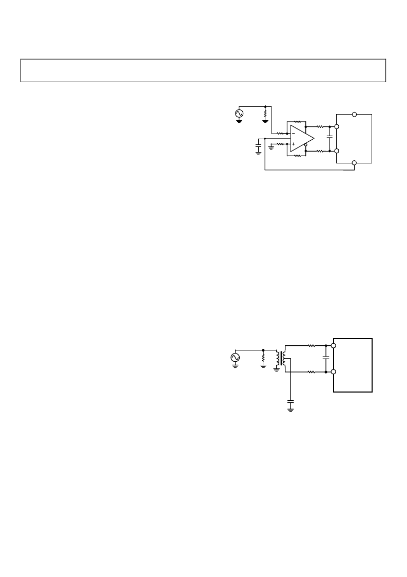
Differential Input Configurations
Optimum performance is achieved while driving the AD9211
in a differential input configuration. For baseband applications,
the AD8138 differential driver provides excellent performance
and a flexible interface to the ADC. The output common-mode
voltage of the AD8138 is easily set to AVDD/2+0.5V, and the
driver can be configured in a Sallen-Key filter topology to
provide band limiting of the input signal.
Figure 8. Differential Input Configuration Using the AD8138
At input frequencies in the second Nyquist zone and above, the
performance of most amplifiers is not adequate to achieve the
true performance of the AD9211. This is especially true in IF
under-sampling applications where frequencies in the 70 MHz
to 100 MHz range are being sampled. For these applications,
differential transformer coupling is the recommended input
configuration. The signal characteristics must be considered
when selecting a transformer. Most RF transformers saturate at
frequencies below a few MHz, and excessive signal power can
also cause core saturation, which leads to distortion.
In any configuration, the value of the shunt capacitor, C, is
dependent on the input frequency and may need to be reduced
or removed.
Figure 9. Differential Transformer—Coupled Configuration
Single-Ended Input Configuration
A single-ended input can provide adequate performance in
cost-sensitive applications. In this configuration, SFDR and
distortion performance degrade due to the large input
common-mode swing. However, if the source impedances
on each input are matched, there should be little effect on
SNR performance. Figure 10 details a typical single-ended
input configuration.
AD9211
VIN+
VIN
–
33
Ω
33
Ω
10pF
49.9
Ω
0.1
μ
F
1.25V p-p
05491-005
AD9211
VIN+
VIN–
CML
AVDD
1V p-p
49.9
Ω
523
Ω
0.1
μ
F
33
Ω
33
Ω
20pF
499
Ω
499
Ω
499
Ω
AD8138
05491-004
相關PDF資料 |
PDF描述 |
|---|---|
| AD9211-170EB | 10-Bit, 170/200/250 MSPS 1.8 V A/D Converter |
| AD9211-200EB | 10-Bit, 170/200/250 MSPS 1.8 V A/D Converter |
| AD9211-250EB | 10-Bit, 170/200/250 MSPS 1.8 V A/D Converter |
| AD9211BCPZ-170 | 10-Bit, 170/200/250 MSPS 1.8 V A/D Converter |
| AD9211BCPZ-200 | 10-Bit, 170/200/250 MSPS 1.8 V A/D Converter |
相關代理商/技術參數(shù) |
參數(shù)描述 |
|---|---|
| AD9211_07 | 制造商:AD 制造商全稱:Analog Devices 功能描述:10-Bit, 200 MSPS/250 MSPS/300 MSPS, 1.8 V Analog-to-Digital Converter |
| AD9211-170EB | 制造商:AD 制造商全稱:Analog Devices 功能描述:10-Bit, 170/200/250 MSPS 1.8 V A/D Converter |
| AD9211-200EB | 制造商:AD 制造商全稱:Analog Devices 功能描述:10-Bit, 170/200/250 MSPS 1.8 V A/D Converter |
| AD9211-200EBZ | 功能描述:BOARD EVAL FOR AD9211-200 RoHS:是 類別:編程器,開發(fā)系統(tǒng) >> 評估板 - 模數(shù)轉(zhuǎn)換器 (ADC) 系列:- 產(chǎn)品培訓模塊:Obsolescence Mitigation Program 標準包裝:1 系列:- ADC 的數(shù)量:1 位數(shù):12 采樣率(每秒):94.4k 數(shù)據(jù)接口:USB 輸入范圍:±VREF/2 在以下條件下的電源(標準):- 工作溫度:-40°C ~ 85°C 已用 IC / 零件:MAX11645 已供物品:板,軟件 |
| AD9211-250EB | 制造商:AD 制造商全稱:Analog Devices 功能描述:10-Bit, 170/200/250 MSPS 1.8 V A/D Converter |
發(fā)布緊急采購,3分鐘左右您將得到回復。