- 您現在的位置:買賣IC網 > PDF目錄373960 > AD9216-105PCB (Analog Devices, Inc.) 10-Bit, 65/80/105 MSPS Dual A/D Converter PDF資料下載
參數資料
| 型號: | AD9216-105PCB |
| 廠商: | Analog Devices, Inc. |
| 英文描述: | 10-Bit, 65/80/105 MSPS Dual A/D Converter |
| 中文描述: | 10位,65/80/105 MSPS雙通道的A / D轉換器 |
| 文件頁數: | 14/20頁 |
| 文件大小: | 298K |
| 代理商: | AD9216-105PCB |
AD9216
Preliminary Technical Data
help reduce the peak transient current required from the output
stage of the driving source. Also, a small shunt capacitor can be
placed across the inputs to provide dynamic charging currents.
This passive network will create a low-pass filter at the ADC’s
input; therefore, the precise values are dependant on the
application. In IF under sampling applications, any shunt
capacitors should be removed. In combination with the driving
source impedance, they would limit the input bandwidth. For
best dynamic performance, the source impedances driving
VIN+ and VIN- should be matched such that common-mode
settling errors are symmetrical. These errors will be reduced by
the common-mode rejection of the ADC.
Rev. PrD
Page 14 of 20
6/15/2004
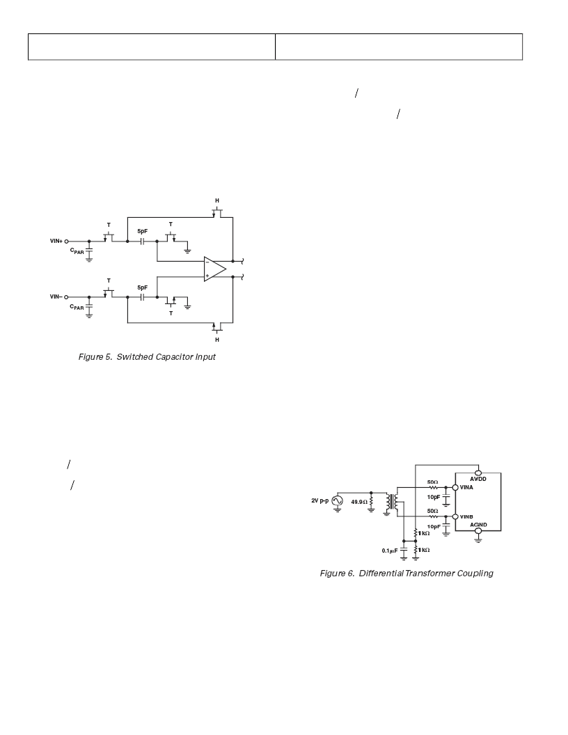
Figure 4.
Switched Capacitor Input
An internal differential reference buffer creates positive and
negative reference voltages, REFT and REFB, respectively, that
define the span of the ADC core. The output common-mode of
the reference buffer is set to midsupply, and the REFT and
REFB voltages and span are defined as follows:
(
REF
V
AVDD
2
1
REFT
+
=
)
(
)
REF
)
=
V
AVDD
REFB
=
2
(
REFT
1
REF
V
2
REFB
2
Span
×
×
=
It can be seen from the equations above that the REFT and
REFB voltages are symmetrical about the mid-supply voltage
and, by definition, the input span is twice the value of the V
REF
voltage.
The internal voltage reference can be pin-strapped to fixed
values of 0.5 V or 1.0 V, or adjusted within the same range as
discussed in the Internal Reference Connection section.
Maximum SNR performance will be achieved with the
AD9216 set to the largest input span of
2 V
. The relative SNR degradation will be 3 dB when
changing from 2 V
P-P
mode to 1 V
P-P
mode.
The SHA may be driven from a source that keeps the signal
peaks within the allowable range for the selected reference
voltage. The minimum and maximum common-mode input
levels are defined as follows:
2
V
(
VCM
REF
MIN
=
)
2
V
AVDD
VCM
REF
MAX
+
=
The minimum common-mode input level allows the AD9216 to
accommodate ground-referenced inputs. Although optimum
performance is achieved with a differential input, a single-
ended source may be driven into VIN+ or VIN- . In this
configuration, one input will accept the signal, while the
opposite input should be set to mid-scale by connecting it to an
appropriate reference. For example, a 2 V
P-P
signal may be
applied to VIN+ while a 1 V reference is applied to VIN- . The
AD9216 will then accept an input signal varying between 2 V
and 0 V. In the single-ended configuration, distortion
performance may degrade significantly as compared to the
differential case. However, the effect will be less noticeable at
lower input frequencies and in the lower speed grade models
(AD9216-65 and AD9216-80).
Differential Input Configurations
As previously detailed, optimum performance will be achieved
while driving the AD9216 in a differential input configuration.
For base band applications, the AD8138 differential driver
provides excellent performance and a flexible interface to the
ADC. The output common-mode voltage of the AD8138 is
easily set to AVDD/2, and the driver can be configured in a
Sallen-Key filter topology to provide band limiting of the input
signal.
At input frequencies in the second Nyquist zone and above, the
performance of most amplifiers will not be adequate to achieve
the true performance of the AD9216. This is especially true in
IF under sampling applications where frequencies in the 70
MHz to 200 MHz range are being sampled. For these
applications, differential transformer coupling is the
recommended input configuration, as shown in Figure 5.
Figure 5.
Differential Transformer Coupling
The signal characteristics must be considered when selecting a
transformer. Most RF transformers will saturate at frequencies
below a few MHz, and excessive signal power can also cause
core saturation, which leads to distortion.
Single-Ended Input Configuration
A single-ended input may provide adequate performance in
AD9216
相關PDF資料 |
PDF描述 |
|---|---|
| AD9216-40PCB | 10-Bit, 65/80/105 MSPS Dual A/D Converter |
| AD9216-65 | 10-Bit, 65/80/105 MSPS Dual A/D Converter |
| AD9216-65PCB | 10-Bit, 65/80/105 MSPS Dual A/D Converter |
| AD9216-80 | 10-Bit, 65/80/105 MSPS Dual A/D Converter |
| AD9216BCP-65 | 10-Bit, 65/80/105 MSPS Dual A/D Converter |
相關代理商/技術參數 |
參數描述 |
|---|---|
| AD9216-105PCBZ | 功能描述:BOARD EVAL FOR AD9216 105MSPS RoHS:是 類別:編程器,開發系統 >> 評估板 - 模數轉換器 (ADC) 系列:- 產品培訓模塊:Obsolescence Mitigation Program 標準包裝:1 系列:- ADC 的數量:1 位數:12 采樣率(每秒):94.4k 數據接口:USB 輸入范圍:±VREF/2 在以下條件下的電源(標準):- 工作溫度:-40°C ~ 85°C 已用 IC / 零件:MAX11645 已供物品:板,軟件 |
| AD9216-40PCB | 制造商:AD 制造商全稱:Analog Devices 功能描述:10-Bit, 65/80/105 MSPS Dual A/D Converter |
| AD9216-65 | 制造商:AD 制造商全稱:Analog Devices 功能描述:10-Bit, 65/80/105 MSPS Dual A/D Converter |
| AD9216-65PCB | 制造商:AD 制造商全稱:Analog Devices 功能描述:10-Bit, 65/80/105 MSPS Dual A/D Converter |
| AD9216-80 | 制造商:AD 制造商全稱:Analog Devices 功能描述:10-Bit, 65/80/105 MSPS Dual A/D Converter |
發布緊急采購,3分鐘左右您將得到回復。