- 您現在的位置:買賣IC網 > PDF目錄373960 > AD9220 (Analog Devices, Inc.) Complete 12-Bit 1.5/3.0/10.0 MSPS Monolithic A/D Converters PDF資料下載
參數資料
| 型號: | AD9220 |
| 廠商: | Analog Devices, Inc. |
| 元件分類: | 串行ADC |
| 英文描述: | Complete 12-Bit 1.5/3.0/10.0 MSPS Monolithic A/D Converters |
| 中文描述: | 完整的12位1.5/3.0/10.0 MSPS的單片的A / D轉換器 |
| 文件頁數: | 20/28頁 |
| 文件大小: | 350K |
| 代理商: | AD9220 |
第1頁第2頁第3頁第4頁第5頁第6頁第7頁第8頁第9頁第10頁第11頁第12頁第13頁第14頁第15頁第16頁第17頁第18頁第19頁當前第20頁第21頁第22頁第23頁第24頁第25頁第26頁第27頁第28頁
AD9221/AD9223/AD9220
REV. D
–20–
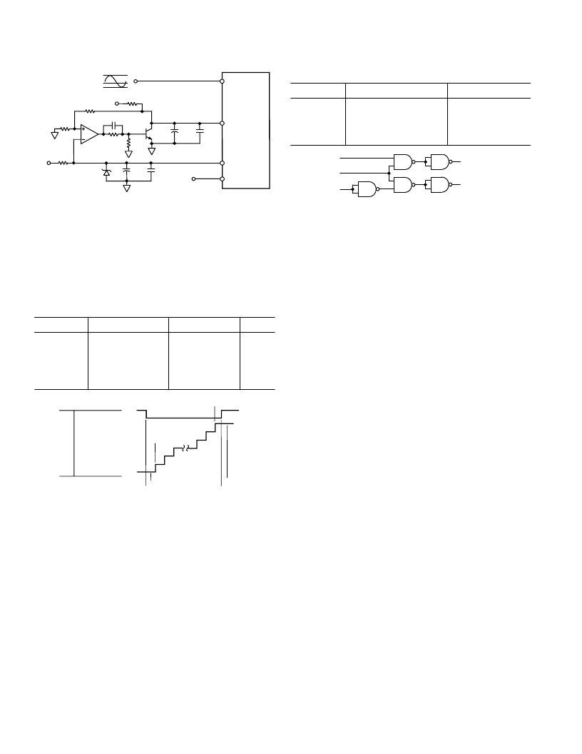
Table V. Out-of-Range Truth Table
OTR
MSB
Analog Input Is
0
0
1
1
0
1
0
1
In Range
In Range
Underrange
Overrange
OVER = “1”
UNDER = “1”
MSB
OTR
MSB
Figure 54. Overrange or Underrange Logic
Digital Output Driver Considerations (DVDD)
The AD9221, AD9223 and AD9220ARS output drivers can be
configured to interface with +5 V or 3.3 V logic families by setting
DVDD to +5 V or 3.3 V respectively. However, the AD9220AR
can only be configured to interface with +5 V logic families. The
AD9221/AD9223/AD9220 output drivers are sized to provide
sufficient output current to drive a wide variety of logic families.
However, large drive currents tend to cause glitches on the
supplies and may affect SINAD performance. Applications
requiring the AD9221/AD9223/AD9220 to drive large capaci-
tive loads or large fanout may require additional decoupling
capacitors on DVDD. In extreme cases, external buffers or
latches may be required.
Clock Input and Considerations
The AD9221/AD9223/AD9220 internal timing uses the two
edges of the clock input to generate a variety of internal timing
signals. The clock input must meet or exceed the minimum
specified pulsewidth high and low (t
CH
and t
CL
) specifications
for the given A/D as defined in the Switching Specifications at
the beginning of the data sheet to meet the rated performance
specifications. For example, the clock input to the AD9220
operating at 10 MSPS may have a duty cycle between 45% to
55% to meet this timing requirement since the minimum specified
t
CH
and t
CL
is 45 ns. For clock rates below 10 MSPS, the duty
cycle may deviate from this range to the extent that both t
CH
and t
CL
are satisfied.
All high speed high resolution A/Ds are sensitive to the quality
of the clock input. The degradation in SNR at a given full-scale
input frequency (f
IN
) due to only aperture jitter (t
A
) can be
calculated with the following equation:
SNR
= 20 log
10
[1/2
π
f
IN
t
A
]
In the equation, the rms aperture jitter, t
A
, represents the root-
sum square of all the jitter sources which include the clock in-
put, analog input signal, and A/D aperture jitter specification.
For example, if a 5 MHz full-scale sine wave is sampled by an
A/D with a total rms jitter of 15 ps, the SNR performance of the
A/D will be limited to 66.5 dB. Undersampling applications are
particularly sensitive to jitter.
The clock input should be treated as an analog signal in cases
where aperture jitter may affect the dynamic range of the
AD9221/AD9223/AD9220. As such, supplies for clock drivers
should be separated from the A/D output driver supplies to
avoid modulating the clock signal with digital noise. Low jitter
crystal controlled oscillators make the best clock sources. If the
3.75V
1.25V
+5V
10
m
F
VINA
VINB
VREF
SENSE
AD9221/
AD9223/
AD9220
+5V
0.1
m
F
316
V
1k
V
0.1
m
F
1/2
OP282
10
m
F
0.1
m
F
7.5k
V
AD1580
1k
V
1k
V
820
V
+5V
2N2222
1.225V
Figure 52. External Reference Using the AD1580 and Low
Impedance Buffer
DIGITAL INPUTS AND OUTPUTS
Digital Outputs
The AD9221/AD9223/AD9220 output data is presented in
positive true straight binary for all input ranges. Table IV indi-
cates the output data formats for various input ranges regardless
of the selected input range. A twos complement output data
format can be created by inverting the MSB.
Table IV. Output Data Format
I
nput (V)
Condition (V)
Digital Output
OTR
VINA –VINB
VINA –VINB
VINA –VINB
VINA –VINB
VINA –VINB
< – VREF
= – VREF
= 0
= + VREF – 1 LSB
≥
+ VREF
0000 0000 0000
0000 0000 0000
1000 0000 0000
1111 1111 1111
1111 1111 1111
1
0
0
0
1
1111 1111 1111
1111 1111 1111
1111 1111 1110
OTR
–FS
+FS
–FS+1/2 LSB
+FS –1/2 LSB
–FS –1/2 LSB
+FS –1 1/2 LSB
0000 0000 0001
0000 0000 0000
0000 0000 0000
1
0
0
0
0
1
OTR DATA OUTPUTS
Figure 53. Output Data Format
Out Of Range (OTR)
An out-of-range condition exists when the analog input voltage
is beyond the input range of the converter. OTR is a digital
output that is updated along with the data output corresponding
to the particular sampled analog input voltage. Hence, OTR has
the same pipeline delay (latency) as the digital data. It is LOW
when the analog input voltage is within the analog input range.
It is HIGH when the analog input voltage exceeds the input
range as shown in Figure 53. OTR will remain HIGH until the
analog input returns within the input range and another conver-
sion is completed. By logical ANDing OTR with the MSB
and its complement, overrange high or underrange low condi-
tions can be detected. Table V is a truth table for the over/
underrange circuit in Figure 54 which uses NAND gates. Sys-
tems requiring programmable gain conditioning of the AD9221/
AD9223/AD9220 input signal can immediately detect an out-
of-range condition, thus eliminating gain selection iterations.
Also, OTR can be used for digital offset and gain calibration.
相關PDF資料 |
PDF描述 |
|---|---|
| AD9223ARS | Complete 12-Bit 1.5/3.0/10.0 MSPS Monolithic A/D Converters |
| AD9220AR | Complete 12-Bit 1.5/3.0/10.0 MSPS Monolithic A/D Converters |
| AD9220ARS | Complete 12-Bit 1.5/3.0/10.0 MSPS Monolithic A/D Converters |
| AD9221 | Complete 12-Bit 1.5/3.0/10.0 MSPS Monolithic A/D Converters |
| AD9221AR | RES, 18.2K, 1/4, 1%, MF |
相關代理商/技術參數 |
參數描述 |
|---|---|
| AD9220AR | 功能描述:IC ADC 12BIT 10MSPS 28-SOIC RoHS:否 類別:集成電路 (IC) >> 數據采集 - 模數轉換器 系列:- 標準包裝:1,000 系列:- 位數:12 采樣率(每秒):300k 數據接口:并聯 轉換器數目:1 功率耗散(最大):75mW 電壓電源:單電源 工作溫度:0°C ~ 70°C 安裝類型:表面貼裝 封裝/外殼:24-SOIC(0.295",7.50mm 寬) 供應商設備封裝:24-SOIC 包裝:帶卷 (TR) 輸入數目和類型:1 個單端,單極;1 個單端,雙極 |
| AD9220AR-REEL | 功能描述:IC ADC 12BIT 10MSPS 28-SOIC RoHS:否 類別:集成電路 (IC) >> 數據采集 - 模數轉換器 系列:- 標準包裝:1,000 系列:- 位數:16 采樣率(每秒):45k 數據接口:串行 轉換器數目:2 功率耗散(最大):315mW 電壓電源:模擬和數字 工作溫度:0°C ~ 70°C 安裝類型:表面貼裝 封裝/外殼:28-SOIC(0.295",7.50mm 寬) 供應商設備封裝:28-SOIC W 包裝:帶卷 (TR) 輸入數目和類型:2 個單端,單極 |
| AD9220ARS | 功能描述:IC ADC 12BIT 10MSPS 28-SSOP RoHS:否 類別:集成電路 (IC) >> 數據采集 - 模數轉換器 系列:- 標準包裝:1,000 系列:- 位數:12 采樣率(每秒):300k 數據接口:并聯 轉換器數目:1 功率耗散(最大):75mW 電壓電源:單電源 工作溫度:0°C ~ 70°C 安裝類型:表面貼裝 封裝/外殼:24-SOIC(0.295",7.50mm 寬) 供應商設備封裝:24-SOIC 包裝:帶卷 (TR) 輸入數目和類型:1 個單端,單極;1 個單端,雙極 |
| AD9220ARS-REEL | 功能描述:IC ADC 12BIT 10MSPS 28-SSOP RoHS:否 類別:集成電路 (IC) >> 數據采集 - 模數轉換器 系列:- 標準包裝:1,000 系列:- 位數:16 采樣率(每秒):45k 數據接口:串行 轉換器數目:2 功率耗散(最大):315mW 電壓電源:模擬和數字 工作溫度:0°C ~ 70°C 安裝類型:表面貼裝 封裝/外殼:28-SOIC(0.295",7.50mm 寬) 供應商設備封裝:28-SOIC W 包裝:帶卷 (TR) 輸入數目和類型:2 個單端,單極 |
| AD9220ARSZ | 功能描述:IC ADC 12BIT 10MSPS 28-SSOP RoHS:是 類別:集成電路 (IC) >> 數據采集 - 模數轉換器 系列:- 標準包裝:1 系列:microPOWER™ 位數:8 采樣率(每秒):1M 數據接口:串行,SPI? 轉換器數目:1 功率耗散(最大):- 電壓電源:模擬和數字 工作溫度:-40°C ~ 125°C 安裝類型:表面貼裝 封裝/外殼:24-VFQFN 裸露焊盤 供應商設備封裝:24-VQFN 裸露焊盤(4x4) 包裝:Digi-Reel® 輸入數目和類型:8 個單端,單極 產品目錄頁面:892 (CN2011-ZH PDF) 其它名稱:296-25851-6 |
發布緊急采購,3分鐘左右您將得到回復。