- 您現在的位置:買賣IC網 > PDF目錄373960 > AD9221 (Analog Devices, Inc.) Complete 12-Bit 1.5/3.0/10.0 MSPS Monolithic A/D Converters PDF資料下載
參數資料
| 型號: | AD9221 |
| 廠商: | Analog Devices, Inc. |
| 元件分類: | 串行ADC |
| 英文描述: | Complete 12-Bit 1.5/3.0/10.0 MSPS Monolithic A/D Converters |
| 中文描述: | 完整的12位1.5/3.0/10.0 MSPS的單片的A / D轉換器 |
| 文件頁數: | 23/28頁 |
| 文件大小: | 350K |
| 代理商: | AD9221 |
第1頁第2頁第3頁第4頁第5頁第6頁第7頁第8頁第9頁第10頁第11頁第12頁第13頁第14頁第15頁第16頁第17頁第18頁第19頁第20頁第21頁第22頁當前第23頁第24頁第25頁第26頁第27頁第28頁
AD9221/AD9223/AD9220
REV. D
–23–
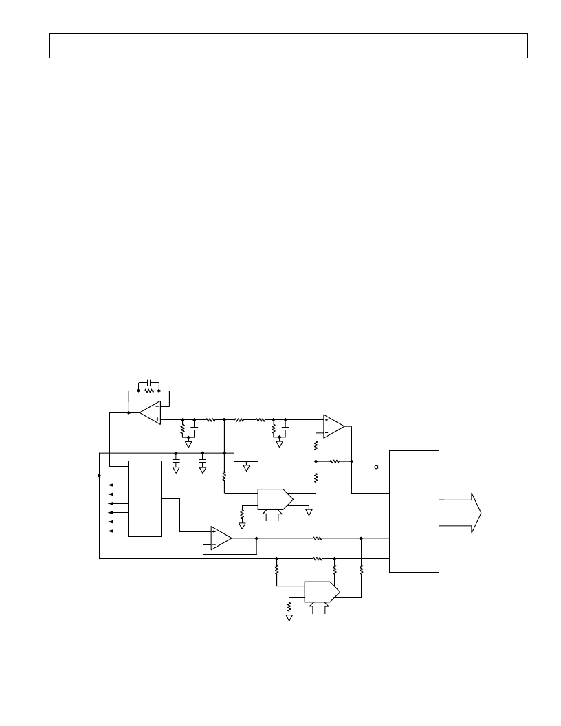
Referring to Figure 61, the AD9221/AD9223/AD9220 is config-
ured for single-ended operation with a 2.5 V p-p input span and
a 2.5 V common-mode voltage using an external, precision 2.5
voltage reference, U1. This configuration and input span allows
the buffer amplifier, U4, to be single supply. Also, it simplifies
the design of the low temperature drift autocalibration circuitry
which uses thin-film resistors for temperature stability and ratio-
metric accuracy. The input of the AD9221/AD9223/AD9220
can be easily configured for a wider span but it should remain
within the input/output swing capabilities of a high speed, rail-
to-rail, single-supply amplifier, U4 (e.g., AD8041).
The gain and offset calibration circuitry is based on two 8-bit,
current-output DAC08s, U3 and U5. The gain calibration
circuitry consisting of U3, and an op amp, U2A, is configured
to provide a low drift nominal 1.25 V reference to the AD9221/
AD9223/AD9220. The resistor values which set the gain cali-
bration range were selected to provide a nominal adjustment
span of
±
128 LSBs with 1 LSB resolution with respect to the
A/D. Note that the bandwidth of the reference is low and, as a
result, it is not possible to change the reference voltage rapidly
in this mode.
The offset calibration circuitry consists of a DAC, U5 and the
buffer amplifier, U4. The DAC is configured for a bipolar ad-
justment span of
±
64 LSB with a 1/2 LSB resolution span with
respect to the AD9221/AD9223/AD9220. Note that both cur-
rent outputs of U5 were configured to provide a bipolar adjust-
ment span. Also, R
C
is used to decouple the output of both
DACs, U3 and U5, from their respective op amps.
The calibration procedure consists of a two step process. First,
the bipolar offset is calibrated by selecting CH2, the 2.5 V sys-
tem reference, of the analog multiplexer and preloading the
DAC, U5, with a midscale code of 1000 0000. If possible, sev-
eral readings of the A/D should be taken and averaged to deter-
mine the required digital offset adjustment code, U5. This
averaged offset code requires an extra bit of resolution since 1
LSB of U5 equates to 1/2 LSB of the AD9221/AD9223/AD9220.
The required offset correction code to U5 can then be deter-
mined. Second, the system gain is calibrated by selecting CH2,
a 1.25 V input which corresponds to –F
S
of the A/D. Before the
value is read, U4 should be preloaded with a code of 00 (Hex).
Several readings can also be taken and averaged to determine
the digital gain adjustment code to U2A. In this case, 1 LSB of
the A/D corresponds to 1 LSB of U4.
Due to the AD9221/AD9223/AD9220’s excellent INL perfor-
mance, a two-point calibration procedure (i.e., –F
S
to midscale)
instead of an endpoint calibration procedure was chosen. Also,
since the bipolar offset is insensitive to any gain adjustment (due
to the differential SHA of the A/D), an iterative calibration
process is not required. The temperature stability of the circuit
is enhanced by selecting a dual precision op amp for U2 (e.g.,
OP293) and low temperature drift, thin film resistors. Note
that this application circuit was not built at the release of this
data sheet. Please consult Analog Devices for application assis-
tance or comments.
1.25k
V
0.1
m
F
10
m
F
2.5k
V
2.5k
V
+5V
U1
REF43
VREF(+)
VREF(–)
U3
DAC08
IOUT
IOUT
0.1
m
F
2.5k
V
0.1
m
F
2.5k
V
0.1
m
F
2.5k
V
162
V
2.5k
V
R
C
100
V
1.1k
V
2
3
39
V
U2A
1.25V
6
39mV
U2B
CH1
CH2
CH3
CH4
CH5
CH6
CH7
CH8
U6
ADG608
1.25V
OUT
VREF(+)
VREF(–)
U5
DAC08
IOUT
IOUT
U4
2.5k
V
R
C
100
V
39
V
AD9221/
AD9223/
AD9220
SENSE
VREF
VINA
VINB
BIT 1 – BIT 12
OTR
2.50V
R
C
100
V
2.5k
V
39
V
Figure 61. Typical Multichannel Data Acquisition System
相關PDF資料 |
PDF描述 |
|---|---|
| AD9221AR | RES, 18.2K, 1/4, 1%, MF |
| AD9221ARS | Complete 12-Bit 1.5/3.0/10.0 MSPS Monolithic A/D Converters |
| AD9223 | Complete 12-Bit 1.5/3.0/10.0 MSPS Monolithic A/D Converters |
| AD9223AR | Complete 12-Bit 1.5/3.0/10.0 MSPS Monolithic A/D Converters |
| AD9224ARS | Complete 12-Bit 40 MSPS Monolithic A/D Converter |
相關代理商/技術參數 |
參數描述 |
|---|---|
| AD9221AR | 功能描述:IC ADC 12BIT 1.5MSPS 28-SOIC RoHS:否 類別:集成電路 (IC) >> 數據采集 - 模數轉換器 系列:- 標準包裝:1,000 系列:- 位數:12 采樣率(每秒):300k 數據接口:并聯 轉換器數目:1 功率耗散(最大):75mW 電壓電源:單電源 工作溫度:0°C ~ 70°C 安裝類型:表面貼裝 封裝/外殼:24-SOIC(0.295",7.50mm 寬) 供應商設備封裝:24-SOIC 包裝:帶卷 (TR) 輸入數目和類型:1 個單端,單極;1 個單端,雙極 |
| AD9221AR-REEL | 功能描述:IC ADC 12BIT 1.5MSPS 28-SOIC RoHS:否 類別:集成電路 (IC) >> 數據采集 - 模數轉換器 系列:- 標準包裝:1,000 系列:- 位數:12 采樣率(每秒):300k 數據接口:并聯 轉換器數目:1 功率耗散(最大):75mW 電壓電源:單電源 工作溫度:0°C ~ 70°C 安裝類型:表面貼裝 封裝/外殼:24-SOIC(0.295",7.50mm 寬) 供應商設備封裝:24-SOIC 包裝:帶卷 (TR) 輸入數目和類型:1 個單端,單極;1 個單端,雙極 |
| AD9221ARS | 功能描述:IC ADC 12BIT 1.5MSPS 28-SSOP RoHS:否 類別:集成電路 (IC) >> 數據采集 - 模數轉換器 系列:- 標準包裝:1,000 系列:- 位數:12 采樣率(每秒):300k 數據接口:并聯 轉換器數目:1 功率耗散(最大):75mW 電壓電源:單電源 工作溫度:0°C ~ 70°C 安裝類型:表面貼裝 封裝/外殼:24-SOIC(0.295",7.50mm 寬) 供應商設備封裝:24-SOIC 包裝:帶卷 (TR) 輸入數目和類型:1 個單端,單極;1 個單端,雙極 |
| AD9221ARS-REEL | 功能描述:IC ADC 12BIT 1.5MSPS 28-SSOP RoHS:否 類別:集成電路 (IC) >> 數據采集 - 模數轉換器 系列:- 標準包裝:1,000 系列:- 位數:12 采樣率(每秒):300k 數據接口:并聯 轉換器數目:1 功率耗散(最大):75mW 電壓電源:單電源 工作溫度:0°C ~ 70°C 安裝類型:表面貼裝 封裝/外殼:24-SOIC(0.295",7.50mm 寬) 供應商設備封裝:24-SOIC 包裝:帶卷 (TR) 輸入數目和類型:1 個單端,單極;1 個單端,雙極 |
| AD9221ARSZ | 功能描述:IC ADC 12BIT 1.5MSPS 28SSOP RoHS:是 類別:集成電路 (IC) >> 數據采集 - 模數轉換器 系列:- 標準包裝:1,000 系列:- 位數:12 采樣率(每秒):300k 數據接口:并聯 轉換器數目:1 功率耗散(最大):75mW 電壓電源:單電源 工作溫度:0°C ~ 70°C 安裝類型:表面貼裝 封裝/外殼:24-SOIC(0.295",7.50mm 寬) 供應商設備封裝:24-SOIC 包裝:帶卷 (TR) 輸入數目和類型:1 個單端,單極;1 個單端,雙極 |
發布緊急采購,3分鐘左右您將得到回復。