- 您現在的位置:買賣IC網 > PDF目錄373960 > AD9221ARS (ANALOG DEVICES INC) Complete 12-Bit 1.5/3.0/10.0 MSPS Monolithic A/D Converters PDF資料下載
參數資料
| 型號: | AD9221ARS |
| 廠商: | ANALOG DEVICES INC |
| 元件分類: | ADC |
| 英文描述: | Complete 12-Bit 1.5/3.0/10.0 MSPS Monolithic A/D Converters |
| 中文描述: | 1-CH 12-BIT FLASH METHOD ADC, PARALLEL ACCESS, PDSO28 |
| 封裝: | MO-150AH, SSOP-28 |
| 文件頁數: | 21/28頁 |
| 文件大小: | 350K |
| 代理商: | AD9221ARS |
第1頁第2頁第3頁第4頁第5頁第6頁第7頁第8頁第9頁第10頁第11頁第12頁第13頁第14頁第15頁第16頁第17頁第18頁第19頁第20頁當前第21頁第22頁第23頁第24頁第25頁第26頁第27頁第28頁
AD9221/AD9223/AD9220
REV. D
–21–
GROUNDING AND DECOUPLING
Analog and Digital Grounding
Proper grounding is essential in any high speed, high resolution
system. Multilayer printed circuit boards (PCBs) are recom-
mended to provide optimal grounding and power schemes. The
use of ground and power planes offers distinct advantages:
1. The minimization of the loop area encompassed by a signal
and its return path.
2. The minimization of the impedance associated with ground
and power paths.
3. The inherent distributed capacitor formed by the power
plane, PCB insulation, and ground plane.
These characteristics result in both a reduction of electro-
magnetic interference (EMI) and an overall improvement in
performance.
It is important to design a layout that prevents noise from coupling
onto the input signal. Digital signals should not be run in paral-
lel with input signal traces and should be routed away from the
input circuitry. While the AD9221/AD9223/AD9220 features
separate analog and digital ground pins, it should be treated as
an analog component.
The AVSS and DVSS pins must be joined
together directly under the AD9221/AD9223/AD9220
. A solid
ground plane under the A/D is acceptable if the power and
ground return currents are managed carefully. Alternatively, the
ground plane under the A/D may contain serrations to
steer
currents in predictable directions where cross-coupling between
analog and digital would otherwise be unavoidable. The
AD9221/AD9223/AD9220/EB ground layout, shown in Figure
65, depicts the serrated type of arrangement. The analog and
digital grounds are connected by a jumper below the A/D.
Analog and Digital Supply Decoupling
The AD9221/AD9223/AD9220 features separate analog and
digital supply and ground pins, helping to minimize digital
corruption of sensitive analog signals. In general, AVDD, the
analog supply, should be decoupled to AVSS, the analog com-
mon, as close to the chip as physically possible. Figure 56
shows the recommended decoupling for the analog supplies;
0.1
μ
F ceramic chip capacitors should provide adequately low
impedance over a wide frequency range. Note that the AVDD
and AVSS pins are co-located on the AD9221/AD9223/AD9220
to simplify the layout of the decoupling capacitors and provide
the shortest possible PCB trace lengths. The AD9221/AD9223/
AD9220/EB power plane layout, shown in Figure 66 depicts a
typical arrangement using a multilayer PCB.
0.1
m
F
AVDD
AVSS
26
AD9221/
AD9223/
AD9220
25
0.1
m
F
AVDD
AVSS
15
16
Figure 56. Analog Supply Decoupling
The CML is an internal analog bias point used internally by the
AD9221/AD9223/AD9220. This pin must be decoupled with
at least a 0.1
μ
F capacitor as shown in Figure 57. The dc level of
clock is generated from another type of source (by gating, divid-
ing, or other method), it should be retimed by the original clock
at the last step.
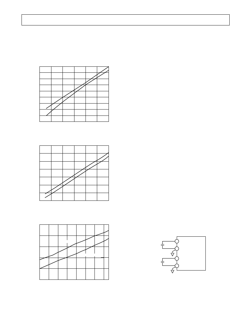
Most of the power dissipated by the AD9221/AD9223/AD9220
is from the analog power supplies. However, lower clock speeds
will reduce digital current slightly. Figure 55 shows the relation-
ship between power and clock rate for each A/D.
CLOCK FREQUENCY – MHz
66
64
56
3.0
P
2.5
62
60
58
5V p-p
2V p-p
54
52
50
48
2.0
1.5
1.0
0.5
Figure 55a. AD9221 Power Consumption vs. Clock
Frequency
CLOCK FREQUENCY – MHz
125
120
105
6
P
5
115
110
5V p-p
2V p-p
100
95
90
4
3
2
1
0
Figure 55b. AD9223 Power Consumption vs. Clock
Frequency
CLOCK FREQUENCY – MHz
300
240
12
P
10
280
260
INPUT = 5V p-p
INPUT = 2V p-p
220
200
8
6
4
2
0
14
Figure 55c. AD9220 Power Consumption vs. Clock
Frequency
相關PDF資料 |
PDF描述 |
|---|---|
| AD9223 | Complete 12-Bit 1.5/3.0/10.0 MSPS Monolithic A/D Converters |
| AD9223AR | Complete 12-Bit 1.5/3.0/10.0 MSPS Monolithic A/D Converters |
| AD9224ARS | Complete 12-Bit 40 MSPS Monolithic A/D Converter |
| AD9224 | Complete 12-Bit 40 MSPS Monolithic A/D Converter |
| AD9224-EB | Complete 12-Bit 40 MSPS Monolithic A/D Converter |
相關代理商/技術參數 |
參數描述 |
|---|---|
| AD9221ARS-REEL | 功能描述:IC ADC 12BIT 1.5MSPS 28-SSOP RoHS:否 類別:集成電路 (IC) >> 數據采集 - 模數轉換器 系列:- 標準包裝:1,000 系列:- 位數:12 采樣率(每秒):300k 數據接口:并聯 轉換器數目:1 功率耗散(最大):75mW 電壓電源:單電源 工作溫度:0°C ~ 70°C 安裝類型:表面貼裝 封裝/外殼:24-SOIC(0.295",7.50mm 寬) 供應商設備封裝:24-SOIC 包裝:帶卷 (TR) 輸入數目和類型:1 個單端,單極;1 個單端,雙極 |
| AD9221ARSZ | 功能描述:IC ADC 12BIT 1.5MSPS 28SSOP RoHS:是 類別:集成電路 (IC) >> 數據采集 - 模數轉換器 系列:- 標準包裝:1,000 系列:- 位數:12 采樣率(每秒):300k 數據接口:并聯 轉換器數目:1 功率耗散(最大):75mW 電壓電源:單電源 工作溫度:0°C ~ 70°C 安裝類型:表面貼裝 封裝/外殼:24-SOIC(0.295",7.50mm 寬) 供應商設備封裝:24-SOIC 包裝:帶卷 (TR) 輸入數目和類型:1 個單端,單極;1 個單端,雙極 |
| AD9221ARSZ-REEL | 功能描述:IC ADC 12BIT 1.5MSPS 28SSOP RoHS:是 類別:集成電路 (IC) >> 數據采集 - 模數轉換器 系列:- 標準包裝:1,000 系列:- 位數:12 采樣率(每秒):300k 數據接口:并聯 轉換器數目:1 功率耗散(最大):75mW 電壓電源:單電源 工作溫度:0°C ~ 70°C 安裝類型:表面貼裝 封裝/外殼:24-SOIC(0.295",7.50mm 寬) 供應商設備封裝:24-SOIC 包裝:帶卷 (TR) 輸入數目和類型:1 個單端,單極;1 個單端,雙極 |
| AD9221ARZ | 功能描述:IC ADC 12BIT 1.5MSPS 28SOIC RoHS:是 類別:集成電路 (IC) >> 數據采集 - 模數轉換器 系列:- 其它有關文件:TSA1204 View All Specifications 標準包裝:1 系列:- 位數:12 采樣率(每秒):20M 數據接口:并聯 轉換器數目:2 功率耗散(最大):155mW 電壓電源:模擬和數字 工作溫度:-40°C ~ 85°C 安裝類型:表面貼裝 封裝/外殼:48-TQFP 供應商設備封裝:48-TQFP(7x7) 包裝:Digi-Reel® 輸入數目和類型:4 個單端,單極;2 個差分,單極 產品目錄頁面:1156 (CN2011-ZH PDF) 其它名稱:497-5435-6 |
| AD9221ARZ-REEL | 功能描述:IC ADC 12BIT 1.5MSPS 28SOIC RoHS:是 類別:集成電路 (IC) >> 數據采集 - 模數轉換器 系列:- 標準包裝:1,000 系列:- 位數:12 采樣率(每秒):300k 數據接口:并聯 轉換器數目:1 功率耗散(最大):75mW 電壓電源:單電源 工作溫度:0°C ~ 70°C 安裝類型:表面貼裝 封裝/外殼:24-SOIC(0.295",7.50mm 寬) 供應商設備封裝:24-SOIC 包裝:帶卷 (TR) 輸入數目和類型:1 個單端,單極;1 個單端,雙極 |
發布緊急采購,3分鐘左右您將得到回復。