- 您現在的位置:買賣IC網 > PDF目錄373961 > AD9229BCP-65 (ANALOG DEVICES INC) Quad 12-Bit, 50/65 MSPS Serial LVDS 3V A/D Converter PDF資料下載
參數資料
| 型號: | AD9229BCP-65 |
| 廠商: | ANALOG DEVICES INC |
| 元件分類: | ADC |
| 英文描述: | Quad 12-Bit, 50/65 MSPS Serial LVDS 3V A/D Converter |
| 中文描述: | 4-CH 12-BIT PROPRIETARY METHOD ADC, SERIAL ACCESS, QCC48 |
| 封裝: | MO-220-VKKD-2, LFCSP-48 |
| 文件頁數: | 11/15頁 |
| 文件大小: | 471K |
| 代理商: | AD9229BCP-65 |
Prelimnary Technical Data
AD9229
THEORY OF OPERATION
Analog Inputs
Rev. PrF |Page 11 of 15
Oct. 6, 2003
For best dynamic performance, the source impedances driving
VIN+ and VIN– should be matched such that common-mode
settling errors are symmetrical. These errors will be reduced by the
common-mode rejection of the A/D.
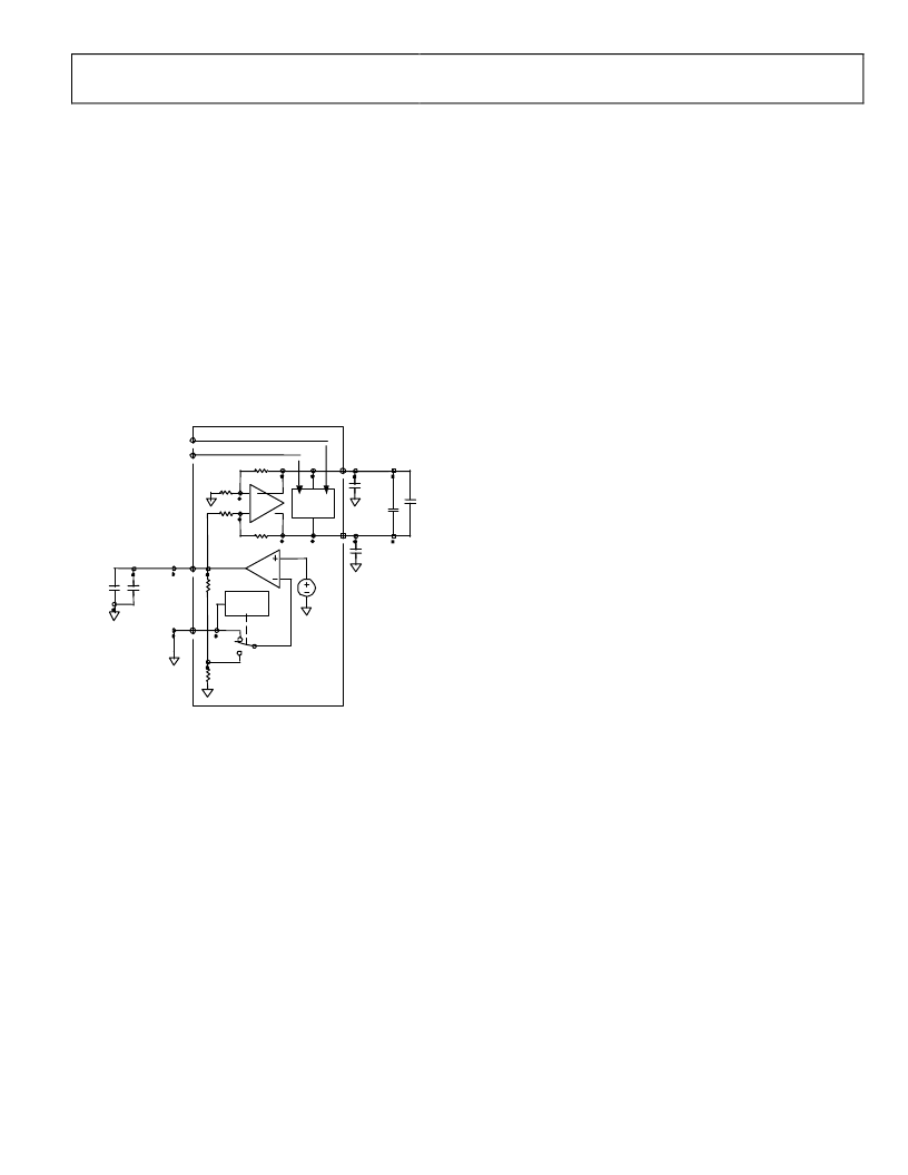
Voltage Reference
The AD9229 has a stable and accurate reference voltage on chip,
which sets the full-scale voltage at the analog input channels.
Internal reference mode is established by grounding the SENSE pin.
(Recommended decoupling capacitors shown below) The internal
reference can be bypassed by setting SENSE to AVDD and driving
VREF with an external 1V reference.
SENSE
ADC
CORE
LOGIC
AD9229
VREF
VINB
VINA
REFB
REFT
0.1
u
F
10
uF
0.1
uF
10
uF
0.1
uF
0.1
uF
0.5V
Internal Reference Mode Connection
Digital Outputs
The AD9229’s differential outputs conform to the ANSI-644 LVDS
standard. To set the LVDS bias current, place a resistor (RSET is
nominally equal to 3.6 k
) to ground at the LVDSBIAS pin. The
RSET resistor current (~ 1.2/RSET) is ratioed on-chip setting the
output current at each output equal to a nominal 3.5 mA. A 100
differential termination resistor placed at the LVDS receiver inputs
results in a nominal 350 mV swing at the receiver.
The AD9229’s LVDS outputs facilitate interfacing with LVDS
receivers in custom ASICs and FPGAs that have LVDS capability
for superior switching performance in noisy environments. Single
point-to-point net topologies are recommended with a 100
termination resistor as close to the receiver as possible. It is
recommended to keep the trace length no longer than 1–2 inches
and to keep differential output trace lengths as equal as possible.
The format of the output data is offset binary.
Timing
Data from each A/D is serialized and provided on a separate
channel.
Two output clocks are provided to assist in capturing data from the
AD9229. The data clock out (DCO) is used to clock the output
data and is equal to 6 times the sample clock frequency. ( 390MHz
for 65MHz input clock) Data is clocked out of the AD9229 on the
rising and falling edges of DCO. The FCO clock signals the start of
a new serial word, the rising edge of FCO occurs at the start of an
MSB.
PLL
The AD9229 contains an internal PLL that is used to generate
internal clocking signals, if the PLL is unlocked, the data outputs
are static.
相關PDF資料 |
PDF描述 |
|---|---|
| AD9229 | Quad 12-Bit, 50/65 MSPS Serial LVDS 3V A/D Converter |
| AD9235 | 12-Bit, 20/40/65 MSPS 3 V A/D Converter |
| AD9235BCP-20 | 12-Bit, 20/40/65 MSPS 3 V A/D Converter |
| AD9235BCP-40 | 12-Bit, 20/40/65 MSPS 3 V A/D Converter |
| AD9235BCP-65 | 12-Bit, 20/40/65 MSPS 3 V A/D Converter |
相關代理商/技術參數 |
參數描述 |
|---|---|
| AD9229BCPZ-50 | 制造商:Analog Devices 功能描述:ADC Quad Pipelined 50Msps 12-bit Serial 48-Pin LFCSP EP |
| AD9229BCPZ-65 | 制造商:Analog Devices 功能描述:ADC Quad Pipelined 65Msps 12-bit Serial 48-Pin LFCSP EP 制造商:Rochester Electronics LLC 功能描述:- Bulk 制造商:Analog Devices 功能描述:IC 12BIT ADC SMD 9229 LFCSP-48 |
| AD9229BCPZRL7-50 | 制造商:Rochester Electronics LLC 功能描述: 制造商:Analog Devices 功能描述: |
| AD9230 | 制造商:AD 制造商全稱:Analog Devices 功能描述:12-Bit, 170/210/250 MSPS 1.8 V A/D Converter |
| AD9230-11 | 制造商:AD 制造商全稱:Analog Devices 功能描述:11-Bit, 200 MSPS, 1.8 V Analog-to-Digital Converter |
發布緊急采購,3分鐘左右您將得到回復。