- 您現在的位置:買賣IC網 > PDF目錄373961 > AD9235 (Analog Devices, Inc.) 12-Bit, 20/40/65 MSPS 3 V A/D Converter PDF資料下載
參數資料
| 型號: | AD9235 |
| 廠商: | Analog Devices, Inc. |
| 元件分類: | ADC |
| 英文描述: | 12-Bit, 20/40/65 MSPS 3 V A/D Converter |
| 中文描述: | 12位,20/40/65MSPS的3V A/D轉換器 |
| 文件頁數: | 13/32頁 |
| 文件大小: | 1181K |
| 代理商: | AD9235 |
第1頁第2頁第3頁第4頁第5頁第6頁第7頁第8頁第9頁第10頁第11頁第12頁當前第13頁第14頁第15頁第16頁第17頁第18頁第19頁第20頁第21頁第22頁第23頁第24頁第25頁第26頁第27頁第28頁第29頁第30頁第31頁第32頁
REV. B
–13–
AD9235
APPLYING THE AD9235
THEORY OF OPERATION
The AD9235 architecture consists of a front-end sample and
hold amplifier (SHA) followed by a pipelined switched capacitor
ADC. The pipelined ADC is divided into three sections, consisting
of a 4-bit first stage followed by eight 1.5-bit stages and a final 3-bit
flash. Each stage provides sufficient overlap to correct for flash
errors in the preceding stages. The quantized outputs from each
stage are combined into a final 12-bit result in the digital correction
logic. The pipelined architecture permits the first stage to operate
on a new input sample while the remaining stages operate on pre-
ceding samples. Sampling occurs on the rising edge of the clock.
Each stage of the pipeline, excluding the last, consists of a low
resolution flash ADC connected to a switched capacitor DAC
and interstage residue amplifier (MDAC). The residue amplifier
magnifies the difference between the reconstructed DAC output and
the flash input for the next stage in the pipeline. One bit of redun-
dancy is used in each stage to facilitate digital correction of flash
errors. The last stage simply consists of a flash ADC.
The input stage contains a differential SHA that can be ac- or
dc-coupled in differential or single-ended modes. The output-
staging block aligns the data, carries out the error correction, and
passes the data to the output buffers. The output buffers are
powered from a separate supply, allowing adjustment of the
output voltage swing. During power-down, the output buffers
go into a high impedance state.
ANALOG INPUT
The analog input to the AD9235 is a differential switched
capacitor SHA that has been designed for optimum performance
while processing a differential input signal. The SHA input can
support a wide common-mode range and maintain excellent
performance, as shown in Figure 7. An input common-mode
voltage of midsupply will minimize signal-dependant errors and
provide optimum performance.
Referring to Figure 6, the clock signal alternatively switches the
SHA between sample mode and hold mode. When the SHA is
switched into sample mode, the signal source must be capable
of charging the sample capacitors and settling within one-half of
a clock cycle. A small resistor in series with each input can help
reduce the peak transient current required from the output stage
of the driving source. Also, a small shunt capacitor can be placed
across the inputs to provide dynamic charging currents. This
passive network will create a low-pass filter at the ADC’s input;
therefore, the precise values are dependant upon the application.
In IF undersampling applications, any shunt capacitors should
be removed. In combination with the driving source impedance,
they would limit the input bandwidth.
For best dynamic performance, the source impedances driving
VIN+ and VIN– should be matched such that common-mode
settling errors are symmetrical. These errors will be reduced by
the common-mode rejection of the ADC.
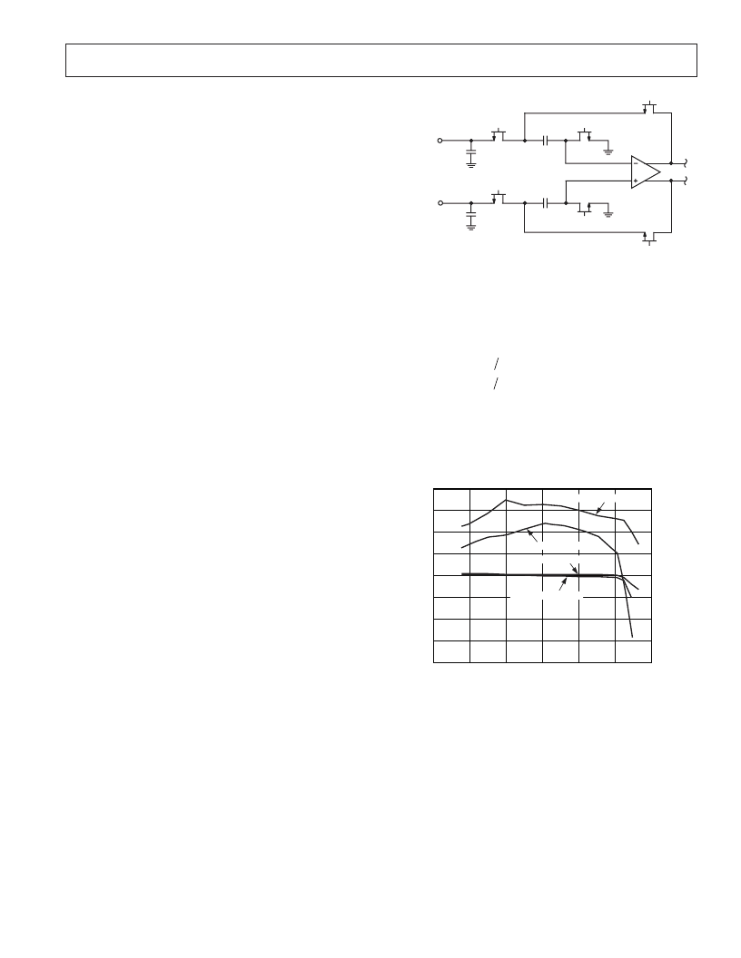
H
H
VIN+
VIN–
C
PAR
C
PAR
T
T
5pF
5pF
T
T
Figure 6. Switched-Capacitor SHA Input
An internal differential reference buffer creates positive and
negative reference voltages, REFT and REFB, respectively, that
define the span of the ADC core. The output common mode of
the reference buffer is set to midsupply, and the REFT and
REFB voltages and span are defined as follows:
REFT
AVDD
=
(
=
(
=
×
(
2
It can be seen from the equations above that the
REFT
and
REFB
voltages are symmetrical about the midsupply voltage
and, by definition, the input span is twice the value of the
VREF voltage.
VREF
REFB
AVDD VREF
Span
REFT
REFB
VREF
+
)
)
)
=
×
1 2
1 2
2
COMMON-MODE LEVEL (V)
S
90
85
75
70
65
50
80
0.0
55
60
0.5
1.0
1.5
2.0
2.5
3.0
T
–90
–85
–80
–75
–70
–65
–60
–55
–50
SNR 35MHz 2V DIFF
THD 35MHz 2V DIFF
THD 2.5MHz 2V DIFF
SNR 2.5MHz 2V DIFF
Figure 7. AD9235-65: SNR, THD vs. Common-Mode Level
The internal voltage reference can be pin-strapped to fixed values
of 0.5 V or 1.0 V, or adjusted within the same range as discussed
in the Internal Reference Connection
section. Maximum SNR
performance will be achieved with the AD9235 set to the largest
input span of 2 V p-p. The relative SNR degradation will be 3 dB
when changing from 2 V p-p mode to 1 V p-p mode.
相關PDF資料 |
PDF描述 |
|---|---|
| AD9235BCP-20 | 12-Bit, 20/40/65 MSPS 3 V A/D Converter |
| AD9235BCP-40 | 12-Bit, 20/40/65 MSPS 3 V A/D Converter |
| AD9235BCP-65 | 12-Bit, 20/40/65 MSPS 3 V A/D Converter |
| AD9235BRU-20 | 12-Bit, 20/40/65 MSPS 3 V A/D Converter |
| AD9235BRU-40 | 12-Bit, 20/40/65 MSPS 3 V A/D Converter |
相關代理商/技術參數 |
參數描述 |
|---|---|
| AD9235-20PCB | 制造商:Analog Devices 功能描述:Development Tools, 12-Bit, 20/40/65MSPS 3V A/D Converter 制造商:Analog Devices 功能描述:DEV TOOLS, 12-BIT, 20/40/65MSPS 3V A/D CNVRTR - Bulk |
| AD9235-40PCB | 制造商:Analog Devices 功能描述:DEV TOOLS, 12-BIT, 20/40/65MSPS 3V A/D CNVRTR - Bulk |
| AD9235-65PCB | 制造商:Analog Devices 功能描述:Development Tools, 12-Bit, 20/40/65MSPS 3V A/D Converter 制造商:Analog Devices 功能描述:DEV TOOLS, 12-BIT, 20/40/65MSPS 3V A/D CNVRTR - Bulk |
| AD9235BCP-20 | 制造商:Analog Devices 功能描述:ADC Single Pipelined 20Msps 12-bit Parallel 32-Pin LFCSP EP 制造商:Analog Devices 功能描述:ADC SGL PIPELINED 20MSPS 12-BIT PARALLEL 32LFCSP EP - Bulk |
| AD9235BCP-20EB | 制造商:Analog Devices 功能描述:EVAL BD FOR 12-BIT, 20/40/65 MSPS ,3V A/D CNVRTR - Bulk |
發布緊急采購,3分鐘左右您將得到回復。