- 您現在的位置:買賣IC網 > PDF目錄373961 > AD9236BRU-80EB (Analog Devices, Inc.) 12-Bit, 80 MSPS, 3V A/D Converter PDF資料下載
參數資料
| 型號: | AD9236BRU-80EB |
| 廠商: | Analog Devices, Inc. |
| 英文描述: | 12-Bit, 80 MSPS, 3V A/D Converter |
| 中文描述: | 12位,80 MSPS的,3V的A / D轉換 |
| 文件頁數: | 18/36頁 |
| 文件大小: | 2056K |
| 代理商: | AD9236BRU-80EB |
第1頁第2頁第3頁第4頁第5頁第6頁第7頁第8頁第9頁第10頁第11頁第12頁第13頁第14頁第15頁第16頁第17頁當前第18頁第19頁第20頁第21頁第22頁第23頁第24頁第25頁第26頁第27頁第28頁第29頁第30頁第31頁第32頁第33頁第34頁第35頁第36頁
AD9236
03066-0-018
10
μ
F+
0.1
μ
F
VREF
SENSE
R2
R1
0.5V
AD9236
VIN–
VIN+
REFT
0.1
μ
F
0.1
μ
F
10
μ
F
0.1
μ
F
REFB
SELECT
LOGIC
ADC
CORE
+
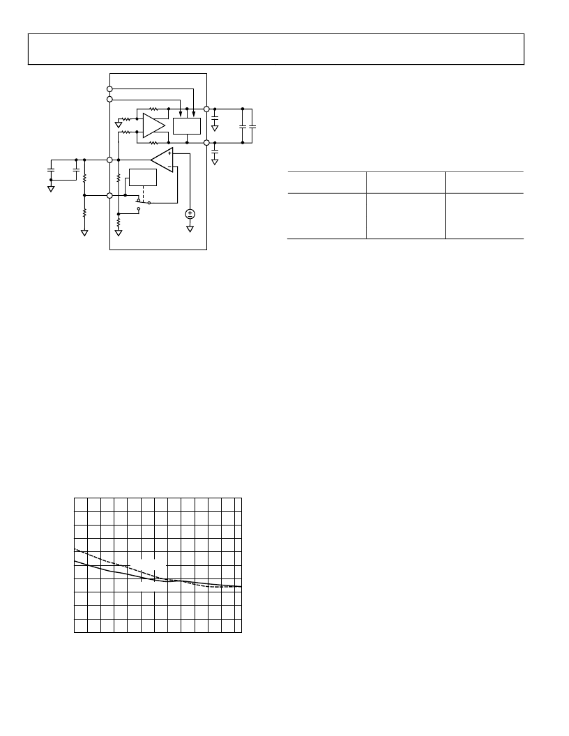
Figure 35. Programmable Reference Configuration
EXTERNAL REFERENCE OPERATION
The use of an external reference may be necessary to enhance
the gain accuracy of the ADC or to improve thermal drift char-
acteristics. When multiple ADCs track one another, a single
reference (internal or external) may be necessary to reduce gain
matching errors to an acceptable level. F
cal drift characteristics of the internal reference in both 1.0 V
and 0.5 V modes.
shows the typi-
igure 36
Figure 36. Typical VREF Drift
When the SENSE pin is tied to AVDD, the internal reference is
disabled, allowing the use of an external reference. An internal
reference buffer loads the external reference with an equivalent
7 k load. The internal buffer still generates the positive and
negative full-scale references, REFT and REFB, for the ADC
core. The input span is always twice the value of the reference
voltage; therefore, the external reference must be limited to a
maximum of 1.0 V.
1.0
V
R
0
–40 –30 –20 –10
0.1
0.2
0.3
0.4
0.5
0.6
0.7
0.8
0.9
0
10
20
30
40
50
60
70
80
TEMPERATURE (
°
C)
03066-0-011
V
REF
= 0.5V
V
REF
= 1.0V
OPERATIONAL MODE SELECTION
As discussed earlier, the AD9236 can output data in either offset
binary or twos complement format. There is also a provision for
enabling or disabling the clock duty cycle stabilizer (DCS). The
MODE pin is a multilevel input that controls the data format
and DCS state. The input threshold values and corresponding
mode selections are outlined in
Table 10
Table 10. Mode Selection
MODE Voltage
Data Format
AVDD
Twos Complement
2/3 AVDD
Twos Complement
1/3 AVDD
Offset Binary
AGND (Default)
Offset Binary
.
Duty Cycle
Stabilizer
Disabled
Enabled
Enabled
Disabled
EVALUATION BOARD
The AD9236 evaluation board provides all of the support cir-
cuitry required to operate the ADC in its various modes and
configurations. Complete schematics and layout plots follow
and demonstrate the proper routing and grounding techniques
that should be applied at the system level.
It is critical that signal sources with very low phase noise (< 1 ps
rms jitter) be used to realize the ultimate performance of the
converter. Proper filtering of the input signal, to remove har-
monics and lower the integrated noise at the input, is also nec-
essary to achieve the specified noise performance.
TSSOP Evaluation Board
Figure 37 shows the typical bench setup used to evaluate the ac
performance of the AD9236. The AD9236 can be driven single-
ended or differentially through an AD8138 driver or a trans-
former. Separate power pins are provided to isolate the DUT
from the support circuitry. Each input configuration can be
selected by proper connection of various jumpers (refer to the
schematics).
The AUXCLK input should be selected in applications requiring
the lowest jitter and SNR performance (i.e., IF undersampling
characterization). It allows the user to apply a clock input signal
that is 4× the target sample rate of the AD9236. A low jitter,
differential divide-by-4 counter, the MC100LVEL33D, provides
a 1× clock output that is subsequently returned back to the CLK
input via JP9. For example, a 260 MHz signal (sinusoid) will be
divided down to a 65 MHz signal for clocking the ADC. Note
that R1 must be removed with the AUXCLK interface. Lower
jitter is often achieved with this interface since many RF signal
generators display improved phase noise at higher output fre-
quencies and the slew rate of the sinusoidal output signal is 4×
that of a 1× signal of equal amplitude.
Rev. A | Page 18 of 36
相關PDF資料 |
PDF描述 |
|---|---|
| AD9238 | 12-Bit, 20/40/65 MSPS Dual A/D Converter |
| AD9238BST-20 | TV07RW21-35SD W/ PC CONT |
| AD9238BST-40 | 12-Bit, 20/40/65 MSPS Dual A/D Converter |
| AD9238BST-65 | 12-Bit, 20/40/65 MSPS Dual A/D Converter |
| AD9238BSTRL-20 | 12-Bit, 20/40/65 MSPS Dual A/D Converter |
相關代理商/技術參數 |
參數描述 |
|---|---|
| AD9236BRURL7-80 | 制造商:Analog Devices 功能描述:ADC Single Pipelined 80Msps 12-bit Parallel 28-Pin TSSOP T/R |
| AD9236BRUZ-80 | 功能描述:IC ADC 12BIT 80MSPS 28TSSOP RoHS:是 類別:集成電路 (IC) >> 數據采集 - 模數轉換器 系列:- 其它有關文件:TSA1204 View All Specifications 標準包裝:1 系列:- 位數:12 采樣率(每秒):20M 數據接口:并聯 轉換器數目:2 功率耗散(最大):155mW 電壓電源:模擬和數字 工作溫度:-40°C ~ 85°C 安裝類型:表面貼裝 封裝/外殼:48-TQFP 供應商設備封裝:48-TQFP(7x7) 包裝:Digi-Reel® 輸入數目和類型:4 個單端,單極;2 個差分,單極 產品目錄頁面:1156 (CN2011-ZH PDF) 其它名稱:497-5435-6 |
| AD9236BRUZRL7-80 | 功能描述:IC ADC 12BIT 80MSPS 28TSSOP RoHS:是 類別:集成電路 (IC) >> 數據采集 - 模數轉換器 系列:- 標準包裝:1 系列:- 位數:14 采樣率(每秒):83k 數據接口:串行,并聯 轉換器數目:1 功率耗散(最大):95mW 電壓電源:雙 ± 工作溫度:0°C ~ 70°C 安裝類型:通孔 封裝/外殼:28-DIP(0.600",15.24mm) 供應商設備封裝:28-PDIP 包裝:管件 輸入數目和類型:1 個單端,雙極 |
| AD9237 | 制造商:AD 制造商全稱:Analog Devices 功能描述:12-Bit, 20 MSPS/40 MSPS/65 MSPS 3 V Low Power A/D Converter |
| AD9237BCP-20EB | 制造商:Analog Devices 功能描述:12 BIT 3V 20 MSPS LOW POWER ADC - Trays |
發布緊急采購,3分鐘左右您將得到回復。