- 您現在的位置:買賣IC網 > PDF目錄373961 > AD9238BST-20 (ANALOG DEVICES INC) TV07RW21-35SD W/ PC CONT PDF資料下載
參數資料
| 型號: | AD9238BST-20 |
| 廠商: | ANALOG DEVICES INC |
| 元件分類: | ADC |
| 英文描述: | TV07RW21-35SD W/ PC CONT |
| 中文描述: | 2-CH 12-BIT FLASH METHOD ADC, PARALLEL ACCESS, PQFP64 |
| 封裝: | MS-026-BBD, LQFP-64 |
| 文件頁數: | 13/24頁 |
| 文件大小: | 1737K |
| 代理商: | AD9238BST-20 |
AD9238
–13–
5pF
5pF
T
T
VIN+
VIN–
C
PAR
T
T
H
H
C
PAR
Figure 5. Switched Capacitor Input
An internal differential reference buffer creates positive and nega-
tive reference voltages, REFT and REFB, respectively, that define
the span of the ADC core. The output common-mode of the
reference buffer is set to midsupply, and the REFT and REFB
voltages and span are defined as follows:
REFT
/
AVDD V
=
(
=
(
=
×
(
2
It can be seen from the equations above that the REFT and REFB
voltages are symmetrical about the midsupply voltage and, by
definition, the input span is twice the value of the V
REF
voltage.
The internal voltage reference can be pin-strapped to fixed values
of 0.5 V or 1.0 V, or adjusted within the same range as discussed
in the Internal Reference Connection section. Maximum SNR
performance will be achieved with the AD9238 set to the largest
input span of 2 V p-p. The relative SNR degradation will be 3 dB
when changing from 2 V p-p mode to 1 V p-p mode.
The SHA may be driven from a source that keeps the signal
peaks within the allowable range for the selected reference volt-
age. The minimum and maximum common-mode input levels
are defined as follows:
VCM
V
VCM
(AVDD V
MAX
=
The minimum common-mode input level allows the AD9238
to accommodate ground-referenced inputs. Although optimum
performance is achieved with a differential input, a single-ended
source may be driven into VIN+ or VIN–. In this configuration,
one input will accept the signal, while the opposite input should
be set to midscale by connecting it to an appropriate reference.
For example, a 2 V p-p signal may be applied to VIN+ while a
1 V reference is applied to VIN–. The AD9238 will then accept
an input signal varying between 2 V and 0 V. In the single-ended
configuration, distortion performance may degrade significantly
as compared to the differential case. However, the effect will be
less noticeable at lower input frequencies and in the lower speed
grade models (AD9238-40 and AD9238-20).
Differential Input Configurations
As previously detailed, optimum performance will be achieved
while driving the AD9238 in a differential input configuration.
For baseband applications, the AD8138 differential driver pro-
vides excellent performance and a flexible interface to the ADC.
REFB
/
AVDD V
Span
REFT
REFB
V
REF
REF
REF
)
)
)
=
×
1 2
1 2
2
)
MIN
REF
REF
=
2
2
The output common-mode voltage of the AD8138 is easily set to
AVDD/2, and the driver can be configured in a Sallen-Key filter
topology to provide band limiting of the input signal.
At input frequencies in the second Nyquist zone and above, the
performance of most amplifiers will not be adequate to achieve
the true performance of the AD9238. This is especially true in
IF undersampling applications where frequencies in the 70 MHz
to 200 MHz range are being sampled. For these applications,
differential transformer coupling is the recommended input con-
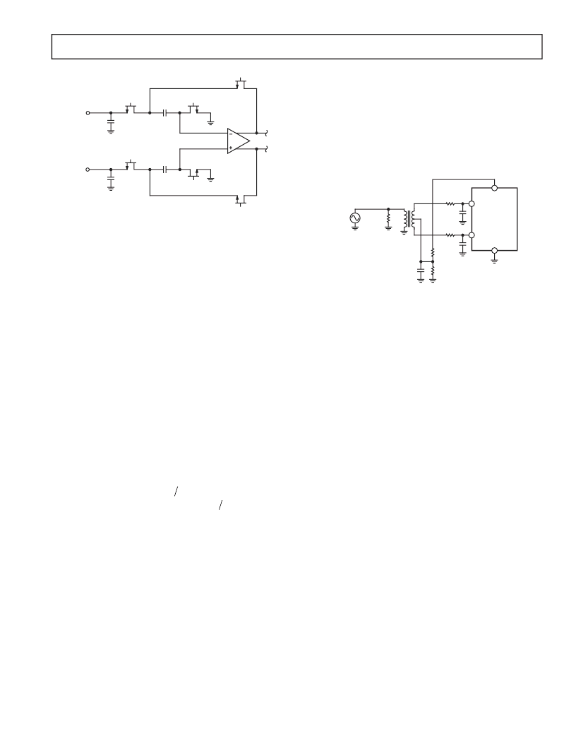
figuration, as shown in Figure 6.
AD9238
VINA
VINB
AVDD
AGND
2V p-p
50
50
10pF
10pF
49.9
1k
1k
0.1
F
Figure 6. Differential Transformer Coupling
The signal characteristics must be considered when selecting a
transformer. Most RF transformers will saturate at frequencies
below a few MHz, and excessive signal power can also cause core
saturation, which leads to distortion.
Single-Ended Input Configuration
A single-ended input may provide adequate performance in
cost-sensitive applications. In this configuration, there will be a
degradation in SFDR and in distortion performance due to the
large input common-mode swing. However, if the source imped-
ances on each input are matched, there should be little effect on
SNR performance.
CLOCK INPUT AND CONSIDERATIONS
Typical high speed ADCs use both clock edges to generate a
variety of internal timing signals, and as a result may be sensitive
to clock duty cycle. Commonly, a 5% tolerance is required on the
clock duty cycle to maintain dynamic performance characteristics.
The AD9238 provides separate clock inputs for each channel. The
optimum performance is achieved with the clocks operated at the
same frequency and phase. Clocking the channels asynchronously
may degrade performance significantly. In some applications, it is
desirable to skew the clock timing of adjacent channels. The AD9238’s
separate clock inputs allow for clock timing skew (typically ±1 ns)
between the channels without significant performance degradation.
The AD9238-65 contains two clock duty cycle stabilizers, one for
each converter, that retime the nonsampling edge, providing an
internal clock with a nominal 50% duty cycle (DCS is not avail-
able on the –40 MSPS or –20 MSPS versions). Input clock rates
of over 40 MHz can use the DCS so that a wide range of input
clock duty cycles can be accommodated. Maintaining a 50% duty
cycle clock is particularly important in high speed applications,
when proper track-and-hold times for the converter are required
to maintain high performance. The DCS can be enabled by tying
the DCS pin high.
The duty cycle stabilizer utilizes a delay locked loop to create the
nonsampling edge. As a result, any changes to the sampling fre-
quency will require approximately 2 μs to 3 μs to allow the DLL
to acquire and settle to the new rate.
REV. A
相關PDF資料 |
PDF描述 |
|---|---|
| AD9238BST-40 | 12-Bit, 20/40/65 MSPS Dual A/D Converter |
| AD9238BST-65 | 12-Bit, 20/40/65 MSPS Dual A/D Converter |
| AD9238BSTRL-20 | 12-Bit, 20/40/65 MSPS Dual A/D Converter |
| AD9238BSTRL-40 | 12-Bit, 20/40/65 MSPS Dual A/D Converter |
| AD9238BSTRL-65 | 12-Bit, 20/40/65 MSPS Dual A/D Converter |
相關代理商/技術參數 |
參數描述 |
|---|---|
| AD9238BST-20PCB | 制造商:Analog Devices 功能描述:Evaluation Board For Ad9238Bst-20 |
| AD9238BST-40 | 功能描述:IC ADC 12BIT DUAL 40MSPS 64-LQFP RoHS:否 類別:集成電路 (IC) >> 數據采集 - 模數轉換器 系列:- 產品培訓模塊:Lead (SnPb) Finish for COTS Obsolescence Mitigation Program 標準包裝:2,500 系列:- 位數:12 采樣率(每秒):3M 數據接口:- 轉換器數目:- 功率耗散(最大):- 電壓電源:- 工作溫度:- 安裝類型:表面貼裝 封裝/外殼:SOT-23-6 供應商設備封裝:SOT-23-6 包裝:帶卷 (TR) 輸入數目和類型:- |
| AD9238BST-40EBZ | 制造商:Analog Devices 功能描述:Evaluation Board For AD9238 Dual A/D Converter ,12-Bit, 20 MSPS/40 MSPS/65 MSPS 制造商:Analog Devices 功能描述:EVAL BD FOR AD9238 DUAL A/D CNVRTR ,12-BIT, 20 MSPS/40 MSPS/ - Bulk |
| AD9238BST-40PCB | 制造商:Analog Devices 功能描述:Evaluation Board For AD9238 Dual A/D Converter ,12-Bit, 20 MSPS/40 MSPS/65 MSPS 制造商:Analog Devices 功能描述:EVAL BD FOR AD9238 DUAL A/D CNVRTR ,12-BIT, 20 MSPS/40 MSPS/ - Bulk |
| AD9238BST-40PCBZ | 制造商:Analog Devices 功能描述:DUAL 12 BIT 3V CMOS 20/40/65 MSPS ADC - Bulk |
發布緊急采購,3分鐘左右您將得到回復。