- 您現(xiàn)在的位置:買賣IC網(wǎng) > PDF目錄373961 > AD9240AS (ANALOG DEVICES INC) Complete 14-Bit, 10 MSPS Monolithic A/D Converter PDF資料下載
參數(shù)資料
| 型號(hào): | AD9240AS |
| 廠商: | ANALOG DEVICES INC |
| 元件分類: | ADC |
| 英文描述: | Complete 14-Bit, 10 MSPS Monolithic A/D Converter |
| 中文描述: | 1-CH 14-BIT FLASH METHOD ADC, PARALLEL ACCESS, QFP44 |
| 封裝: | MS-022AB-1, MQFP-44 |
| 文件頁數(shù): | 19/24頁 |
| 文件大小: | 328K |
| 代理商: | AD9240AS |
AD9240
REV. A
–19–
Table V. Out-of-Range Truth Table
OTR
MSB
Analog Input Is
0
0
1
1
0
1
0
1
In Range
In Range
Underrange
Overrange
OVER = “1”
UNDER = “1”
MSB
OTR
MSB
Figure 46. Overrange or Underrange Logic
Digital Output Driver Considerations (DRVDD)
The AD9240 output drivers can be configured to interface with
+5 V or 3.3 V logic families by setting DRVDD to +5 V or 3.3 V
respectively. The AD9240 output drivers are sized to provide
sufficient output current to drive a wide variety of logic families;
large drive currents tend to cause glitches on the supplies and may
affect SINAD performance. Applications requiring the AD9240 to
drive large capacitive loads or large fanout may require additional
decoupling capacitors on DRVDD. In extreme cases, external
buffers or latches may be required.
Clock Input and Considerations
The AD9240 internal timing uses the two edges of the clock
input to generate a variety of internal timing signals. The clock
input must meet or exceed the minimum specified pulsewidth
high and low (t
CH
and t
CL
) specifications for the given A/D, as
defined in the Switching Specifications at the beginning of the
data sheet, to meet the rated performance specifications. For
example, the clock input to the AD9240 operating at 10 MSPS
may have a duty cycle between 45% to 55% to meet this timing
requirement since the minimum specified t
CH
and t
CL
is 45 ns.
For clock rates below 10 MSPS, the duty cycle may deviate
from this range to the extent that both t
CH
and t
CL
are satisfied.
All high speed high resolution A/Ds are sensitive to the quality
of the clock input. The degradation in SNR at a given full-scale
input frequency (f
IN
), due only to aperture jitter (t
A
), can be
calculated with the following equation:
SNR
= 20 log
10
[1/(2
π
f
IN
t
A
)
]
In the equation, the rms aperture jitter, t
A
, represents the root-
sum square of all the jitter sources, which include the clock
input, analog input signal and A/D aperture jitter specification.
For example, if a 5.0 MHz full-scale sine wave is sampled by an
A/D with a total rms jitter of 15 ps, the SNR performance of the
A/D will be limited to 66.5 dB. Undersampling applications are
particularly sensitive to jitter.
The clock input should be treated as an analog signal in cases
where aperture jitter may affect the dynamic range of the
AD9240. As such, supplies for clock drivers should be separated
from the A/D output driver supplies to avoid modulating the
clock signal with digital noise. Low jitter crystal controlled oscil-
lators make the best clock sources. If the clock is generated from
another type of source (by gating, dividing or other method), it
should be retimed by the original clock at the last step.
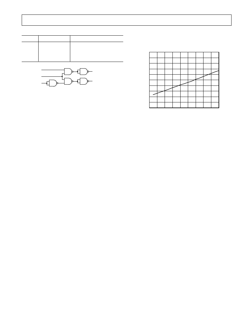
Most of the power dissipated by the AD9240 is from the analog
power supply; however, lower clock speeds will reduce digital
current slightly. Figure 47 shows the relationship between power
and clock rate.
CLOCK FREQUENCY – MHz
400
2002
20
4
6
8
10
12
14
16
18
380
300
260
240
220
360
340
280
320
P
Figure 47. Power Consumption vs. Clock Frequency
(R
BIAS
= 2 k
)
GROUNDING AND DECOUPLING
Analog and Digital Grounding
Proper grounding is essential in any high speed, high resolution
system. Multilayer printed circuit boards (PCBs) are recom-
mended to provide optimal grounding and power schemes. The
use of ground and power planes offers distinct advantages:
1. The minimization of the loop area encompassed by a signal
and its return path.
2. The minimization of the impedance associated with ground
and power paths.
3. The inherent distributed capacitor formed by the power
plane, PCB insulation and ground plane.
These characteristics result in both a reduction of electro-
magnetic interference (EMI) and an overall improvement in
performance.
It is important to design a layout that prevents noise from coupling
onto the input signal. Digital signals should not be run in paral-
lel with input signal traces and should be routed away from the
input circuitry. While the AD9240 features separate analog and
digital ground pins, it should be treated as an analog component.
The AVSS, DVSS and DRVSS pins must be joined together
directly under the AD9240. A solid ground plane under the A/D
is acceptable if the power and ground return currents are care-
fully managed. Alternatively, the ground plane under the A/D
may contain serrations to
steer
currents in predictable directions
where cross-coupling between analog and digital would other-
wise be unavoidable. The AD9240/EB ground layout, shown in
Figure
57, depicts the serrated type of arrangement. The analog
and digital grounds are connected by a jumper below the A/D.
相關(guān)PDF資料 |
PDF描述 |
|---|---|
| AD9240EB | Complete 14-Bit, 10 MSPS Monolithic A/D Converter |
| AD9241 | Complete 14-Bit, 1.25 MSPS Monolithic A/D Converter |
| AD9241AS | RES., MF, 2K, 1%, 1/4W |
| AD9241EB | Complete 14-Bit, 1.25 MSPS Monolithic A/D Converter |
| AD9243 | Complete 14-Bit, 3.0 MSPS Monolithic A/D Converter |
相關(guān)代理商/技術(shù)參數(shù) |
參數(shù)描述 |
|---|---|
| AD9240ASRL | 功能描述:IC ADC 14BIT 10MSPS 44-MQFP RoHS:否 類別:集成電路 (IC) >> 數(shù)據(jù)采集 - 模數(shù)轉(zhuǎn)換器 系列:- 標(biāo)準(zhǔn)包裝:1 系列:- 位數(shù):14 采樣率(每秒):83k 數(shù)據(jù)接口:串行,并聯(lián) 轉(zhuǎn)換器數(shù)目:1 功率耗散(最大):95mW 電壓電源:雙 ± 工作溫度:0°C ~ 70°C 安裝類型:通孔 封裝/外殼:28-DIP(0.600",15.24mm) 供應(yīng)商設(shè)備封裝:28-PDIP 包裝:管件 輸入數(shù)目和類型:1 個(gè)單端,雙極 |
| AD9240ASZ | 功能描述:IC ADC 14BIT 10MSPS 44-MQFP RoHS:是 類別:集成電路 (IC) >> 數(shù)據(jù)采集 - 模數(shù)轉(zhuǎn)換器 系列:- 標(biāo)準(zhǔn)包裝:1 系列:microPOWER™ 位數(shù):8 采樣率(每秒):1M 數(shù)據(jù)接口:串行,SPI? 轉(zhuǎn)換器數(shù)目:1 功率耗散(最大):- 電壓電源:模擬和數(shù)字 工作溫度:-40°C ~ 125°C 安裝類型:表面貼裝 封裝/外殼:24-VFQFN 裸露焊盤 供應(yīng)商設(shè)備封裝:24-VQFN 裸露焊盤(4x4) 包裝:Digi-Reel® 輸入數(shù)目和類型:8 個(gè)單端,單極 產(chǎn)品目錄頁面:892 (CN2011-ZH PDF) 其它名稱:296-25851-6 |
| AD9240ASZRL | 功能描述:IC ADC 14BIT 10MSPS 44-MQFP TR RoHS:是 類別:集成電路 (IC) >> 數(shù)據(jù)采集 - 模數(shù)轉(zhuǎn)換器 系列:- 標(biāo)準(zhǔn)包裝:1 系列:- 位數(shù):14 采樣率(每秒):83k 數(shù)據(jù)接口:串行,并聯(lián) 轉(zhuǎn)換器數(shù)目:1 功率耗散(最大):95mW 電壓電源:雙 ± 工作溫度:0°C ~ 70°C 安裝類型:通孔 封裝/外殼:28-DIP(0.600",15.24mm) 供應(yīng)商設(shè)備封裝:28-PDIP 包裝:管件 輸入數(shù)目和類型:1 個(gè)單端,雙極 |
| AD9240EB | 制造商:AD 制造商全稱:Analog Devices 功能描述:Complete 14-Bit, 10 MSPS Monolithic A/D Converter |
| AD9240-EB | 制造商:Analog Devices 功能描述: |
發(fā)布緊急采購,3分鐘左右您將得到回復(fù)。