- 您現(xiàn)在的位置:買(mǎi)賣(mài)IC網(wǎng) > PDF目錄373961 > AD9241AS (ANALOG DEVICES INC) RES., MF, 2K, 1%, 1/4W PDF資料下載
參數(shù)資料
| 型號(hào): | AD9241AS |
| 廠商: | ANALOG DEVICES INC |
| 元件分類(lèi): | ADC |
| 英文描述: | RES., MF, 2K, 1%, 1/4W |
| 中文描述: | 1-CH 14-BIT FLASH METHOD ADC, PARALLEL ACCESS, PQFP44 |
| 封裝: | METRIC, QFP-44 |
| 文件頁(yè)數(shù): | 17/24頁(yè) |
| 文件大小: | 495K |
| 代理商: | AD9241AS |
第1頁(yè)第2頁(yè)第3頁(yè)第4頁(yè)第5頁(yè)第6頁(yè)第7頁(yè)第8頁(yè)第9頁(yè)第10頁(yè)第11頁(yè)第12頁(yè)第13頁(yè)第14頁(yè)第15頁(yè)第16頁(yè)當(dāng)前第17頁(yè)第18頁(yè)第19頁(yè)第20頁(yè)第21頁(yè)第22頁(yè)第23頁(yè)第24頁(yè)
AD9241
REV. 0
–17–
deliberately left small to minimize the reference noise contribu-
tion. As a result, it is not possible to change the reference volt-
age rapidly in this mode without removing the CAPT/CAPB
Decoupling Network and driving these pins directly.
Variable Input Span with V
CM
= 2.5 V
Figure 39 shows an example of the AD9241 configured for an
input span of 2
×
VREF centered at 2.5 V. An external 2.5 V
reference drives the VINB pin thus setting the common-mode
voltage at 2.5 V. The input span can be independently set by a
voltage divider consisting of R1 and R2, which generates the
VREF signal. A1 buffers this resistor network and drives VREF.
Choose this op amp based on accuracy requirements. It is
essential that a minimum of a 10
μ
F capacitor in parallel with a
0.1
μ
F low inductance ceramic capacitor decouple the reference
output to ground.
2.5V+VREF
2.5V–VREF
2.5V
+5V
0.1μF
22μF
VINA
VINB
VREF
SENSE
AD9241
+5V
R2
0.1μF
A1
R1
0.1μF
2.5V
REF
Figure 39. External Reference, V
CM
= 2.5 V (2.5 V on VINB,
Resistor Divider to Make VREF)
Single-Ended Input with 0 to 2
3
VREF Range
Figure 40 shows an example of an external reference driving
both VINB and VREF. In this case, both the common mode
voltage and input span are directly dependent on the value of
VREF. More specifically, the common-mode voltage is equal to
VREF while the input span is equal to 2
×
VREF. Thus, the
valid input range extends from 0 to 2
×
VREF. For example, if
the REF191, a 2.048 external reference, was selected, the valid
input range extends from 0 V to 4.096 V. In this case, 1 LSB of
the AD9241 corresponds to 0.250 mV. It is essential that a
minimum of a 10
μ
F capacitor in parallel with a 0.1
μ
F low induc-
tance ceramic capacitor decouple the reference output to ground.
2xREF
0V
+5V
10μF
VINA
VINB
VREF
SENSE
AD9241
+5V
0.1μF
VREF
0.1μF
0.1μF
Figure 40. Input Range = 0 V to 2
×
VREF
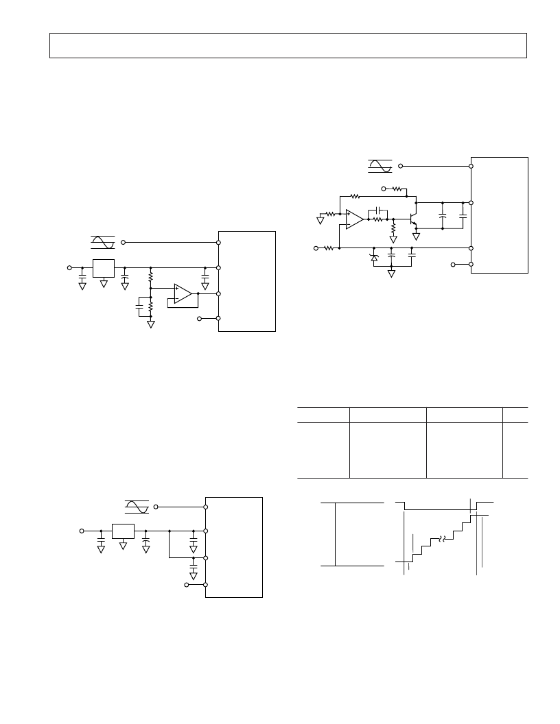
Low Cost/Power Reference
The external reference circuit shown in Figure 41 uses a low
cost 1.225 V external reference (e.g., AD580 or AD1580) along
with an op amp and transistor. The 2N2222 transistor acts in
conjunction with 1/2 of an OP282 to provide a very low imped-
ance drive for VINB. The selected op amp need not be a high
speed op amp and may be selected based on cost, power and
accuracy.
3.75V
1.25V
+5V
10μF
VINA
VINB
VREF
SENSE
AD9241
+5V
0.1μF
316
1k
0.1μF
1/2
OP282
10μF
0.1μF
7.5k
AD1580
1k
1k
820
+5V
2N2222
1.225V
Figure 41. External Reference Using the AD1580 and Low
Impedance Buffer
DIGITAL INPUTS AND OUTPUTS
Digital Outputs
The AD9241 output data is presented in positive true straight
binary for all input ranges. Table IV indicates the output data
formats for various input ranges, regardless of the selected input
range. A twos-complement output data format can be created
by inverting the MSB.
Table IV. Output Data Format
Input (V)
Condition (V)
Digital Output
OTR
VINA –VINB
VINA –VINB
VINA –VINB
VINA –VINB
VINA –VINB
< – VREF
= – VREF
= 0
= + VREF – 1 LSB 11 1111 1111 1111 0
≥
+ VREF
11 1111 1111 1111 1
00 0000 0000 0000 1
00 0000 0000 0000 0
10 0000 0000 0000 0
111111 1111 1111
111111 1111 1111
111111 1111 1110
OTR
–FS
+FS
–FS+1/2 LSB
+FS –1/2 LSB
–FS –1/2 LSB
+FS –1 1/2 LSB
000000 0000 0001
000000 0000 0000
000000 0000 0000
1
0
0
0
0
1
OTR DATA OUTPUTS
Figure 42. Output Data Format
Out Of Range (OTR)
An out-of-range condition exists when the analog input voltage
is beyond the input range of the converter. OTR is a digital
output that is updated along with the data output corresponding
to the particular sampled analog input voltage. Hence, OTR has
the same pipeline delay (latency) as the digital data. It is LOW
when the analog input voltage is within the analog input range.
相關(guān)PDF資料 |
PDF描述 |
|---|---|
| AD9241EB | Complete 14-Bit, 1.25 MSPS Monolithic A/D Converter |
| AD9243 | Complete 14-Bit, 3.0 MSPS Monolithic A/D Converter |
| AD9243AS | Complete 14-Bit, 3.0 MSPS Monolithic A/D Converter |
| AD9243EB | Complete 14-Bit, 3.0 MSPS Monolithic A/D Converter |
| AD9243* | 14-Bit Rail-to-Rail DACs with I2C Interface; Package: DFN; No of Pins: 10; Temperature Range: 0°C to +70°C |
相關(guān)代理商/技術(shù)參數(shù) |
參數(shù)描述 |
|---|---|
| AD9241ASRL | 制造商:Analog Devices 功能描述:ADC Single Pipelined 1.25Msps 14-bit Parallel 44-Pin MQFP T/R |
| AD9241ASZ | 功能描述:IC ADC 14BIT 1.25MSPS 44-MQFP RoHS:是 類(lèi)別:集成電路 (IC) >> 數(shù)據(jù)采集 - 模數(shù)轉(zhuǎn)換器 系列:- 標(biāo)準(zhǔn)包裝:1 系列:microPOWER™ 位數(shù):8 采樣率(每秒):1M 數(shù)據(jù)接口:串行,SPI? 轉(zhuǎn)換器數(shù)目:1 功率耗散(最大):- 電壓電源:模擬和數(shù)字 工作溫度:-40°C ~ 125°C 安裝類(lèi)型:表面貼裝 封裝/外殼:24-VFQFN 裸露焊盤(pán) 供應(yīng)商設(shè)備封裝:24-VQFN 裸露焊盤(pán)(4x4) 包裝:Digi-Reel® 輸入數(shù)目和類(lèi)型:8 個(gè)單端,單極 產(chǎn)品目錄頁(yè)面:892 (CN2011-ZH PDF) 其它名稱(chēng):296-25851-6 |
| AD9241ASZRL | 功能描述:IC ADC 14BIT SGL 1.25MSPS 44MQFP RoHS:是 類(lèi)別:集成電路 (IC) >> 數(shù)據(jù)采集 - 模數(shù)轉(zhuǎn)換器 系列:- 標(biāo)準(zhǔn)包裝:1,000 系列:- 位數(shù):12 采樣率(每秒):300k 數(shù)據(jù)接口:并聯(lián) 轉(zhuǎn)換器數(shù)目:1 功率耗散(最大):75mW 電壓電源:單電源 工作溫度:0°C ~ 70°C 安裝類(lèi)型:表面貼裝 封裝/外殼:24-SOIC(0.295",7.50mm 寬) 供應(yīng)商設(shè)備封裝:24-SOIC 包裝:帶卷 (TR) 輸入數(shù)目和類(lèi)型:1 個(gè)單端,單極;1 個(gè)單端,雙極 |
| AD9241EB | 制造商:AD 制造商全稱(chēng):Analog Devices 功能描述:Complete 14-Bit, 1.25 MSPS Monolithic A/D Converter |
| AD9241-EB | 制造商:Analog Devices 功能描述:Evaluation Board For AD9241 制造商:Analog Devices 功能描述:EVAL BD FOR AD9241 - Bulk |
發(fā)布緊急采購(gòu),3分鐘左右您將得到回復(fù)。