- 您現在的位置:買賣IC網 > PDF目錄373961 > AD9243 (Analog Devices, Inc.) Complete 14-Bit, 3.0 MSPS Monolithic A/D Converter PDF資料下載
參數資料
| 型號: | AD9243 |
| 廠商: | Analog Devices, Inc. |
| 英文描述: | Complete 14-Bit, 3.0 MSPS Monolithic A/D Converter |
| 中文描述: | 完整的14位,3.0 MSPS的單片機的A / D轉換器 |
| 文件頁數: | 18/24頁 |
| 文件大小: | 545K |
| 代理商: | AD9243 |
AD9243
REV. A
–18–
until the analog input returns within the input range and an-
other conversion is completed. By logical ANDing OTR with
the MSB and its complement, overrange high or underrange low
conditions can be detected. Table V is a truth table for the over/
underrange circuit in Figure 43 which uses NAND gates. Sys-
tems requiring programmable gain conditioning of the AD9243
input signal can immediately detect an out-of-range condition,
thus eliminating gain selection iterations. Also, OTR can be
used for digital offset and gain calibration.
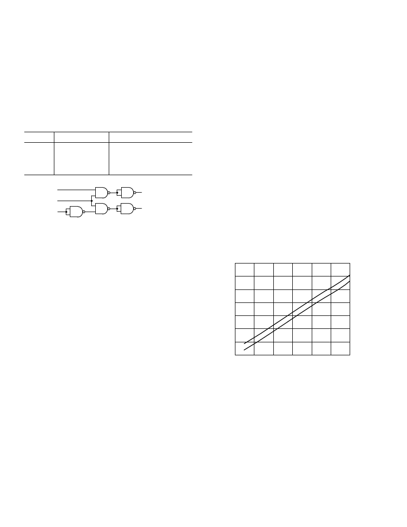
Table V. Out-of-Range Truth Table
OTR
MSB
Analog Input Is
0
0
1
1
0
1
0
1
In Range
In Range
Underrange
Overrange
OVER = “1”
UNDER = “1”
MSB
OTR
MSB
Figure 43. Overrange or Underrange Logic
Digital Output Driver Considerations (DRVDD)
The AD9243 output drivers can be configured to interface with
+5 V or 3.3 V logic families by setting DRVDD to +5 V or 3.3 V
respectively. The AD9243 output drivers are sized to provide
sufficient output current to drive a wide variety of logic families.
However, large drive currents tend to cause glitches on the
supplies and may affect SINAD performance. Applications requir-
ing the AD9243 to drive large capacitive loads or large fanout
may require additional decoupling capacitors on DRVDD. In
extreme cases, external buffers or latches may be required.
Clock Input and Considerations
The AD9243 internal timing uses the two edges of the clock
input to generate a variety of internal timing signals. The clock
input must meet or exceed the minimum specified pulsewidth
high and low (t
CH
and t
CL
) specifications for the given A/D as
defined in the Switching Specifications at the beginning of the
data sheet to meet the rated performance specifications. For
example, the clock input to the AD9243 operating at 3 MSPS
may have a duty cycle between 45% to 55% to meet this timing
requirement since the minimum specified t
CH
and t
CL
is 150 ns.
For clock rates below 3 MSPS, the duty cycle may deviate from
this range to the extent that both t
CH
and t
CL
are satisfied.
All high speed high resolution A/Ds are sensitive to the quality
of the clock input. The degradation in SNR at a given full-scale
input frequency (f
IN
) due to only aperture jitter (t
A
) can be
calculated with the following equation:
SNR
= 20 log
10
[1/(2
π
f
IN
t
A
)
]
In the equation, the rms aperture jitter, t
A
, represents the root-
sum square of all the jitter sources which include the clock in-
put, analog input signal, and A/D aperture jitter specification.
For example, if a 1.5 MHz full-scale sine wave is sampled by an
A/D with a total rms jitter of 15 ps, the SNR performance of the
A/D will be limited to 77 dB. Undersampling applications are
particularly sensitive to jitter.
The clock input should be treated as an analog signal in cases
where aperture jitter may affect the dynamic range of the
AD9243. As such, supplies for clock drivers should be separated
from the A/D output driver supplies to avoid modulating the
clock signal with digital noise. Low jitter crystal controlled
oscillators make the best clock sources. If the clock is generated
from another type of source (by gating, dividing, or other method),
it should be retimed by the original clock at the last step.
Most of the power dissipated by the AD9243 is from the analog
power supply. However, lower clock speeds will reduce digital
current slightly. Figure 44 shows the relationship between power
and clock rate.
CLOCK FREQUENCY – MHz
125
120
105
6
P
5
115
110
5V p-p
2V p-p
100
95
90
4
3
2
1
0
Figure 44. AD9243 Power Consumption vs. Clock
Frequency
相關PDF資料 |
PDF描述 |
|---|---|
| AD9243AS | Complete 14-Bit, 3.0 MSPS Monolithic A/D Converter |
| AD9243EB | Complete 14-Bit, 3.0 MSPS Monolithic A/D Converter |
| AD9243* | 14-Bit Rail-to-Rail DACs with I2C Interface; Package: DFN; No of Pins: 10; Temperature Range: 0°C to +70°C |
| AD9244 | 14-Bit, 40/65 MSPS Monolithic A/D Converter |
| AD9244-40PCB | 14-Bit, 40/65 MSPS Monolithic A/D Converter |
相關代理商/技術參數 |
參數描述 |
|---|---|
| AD9243AS | 制造商:Analog Devices 功能描述:ADC Single Pipelined 3Msps 14-bit Parallel 44-Pin MQFP 制造商:Analog Devices 功能描述:IC 14-BIT ADC |
| AD9243ASRL | 制造商:Analog Devices 功能描述:ADC Single Pipelined 3Msps 14-bit Parallel 44-Pin MQFP T/R |
| AD9243ASZ | 功能描述:IC ADC 14BIT 3MSPS 44-MQFP RoHS:是 類別:集成電路 (IC) >> 數據采集 - 模數轉換器 系列:- 標準包裝:1 系列:microPOWER™ 位數:8 采樣率(每秒):1M 數據接口:串行,SPI? 轉換器數目:1 功率耗散(最大):- 電壓電源:模擬和數字 工作溫度:-40°C ~ 125°C 安裝類型:表面貼裝 封裝/外殼:24-VFQFN 裸露焊盤 供應商設備封裝:24-VQFN 裸露焊盤(4x4) 包裝:Digi-Reel® 輸入數目和類型:8 個單端,單極 產品目錄頁面:892 (CN2011-ZH PDF) 其它名稱:296-25851-6 |
| AD9243ASZRL | 功能描述:IC ADC 14BIT SGL 3MSPS 44MQFP RoHS:是 類別:集成電路 (IC) >> 數據采集 - 模數轉換器 系列:- 標準包裝:1,000 系列:- 位數:12 采樣率(每秒):300k 數據接口:并聯 轉換器數目:1 功率耗散(最大):75mW 電壓電源:單電源 工作溫度:0°C ~ 70°C 安裝類型:表面貼裝 封裝/外殼:24-SOIC(0.295",7.50mm 寬) 供應商設備封裝:24-SOIC 包裝:帶卷 (TR) 輸入數目和類型:1 個單端,單極;1 個單端,雙極 |
發布緊急采購,3分鐘左右您將得到回復。