- 您現在的位置:買賣IC網 > PDF目錄373961 > AD9243AS (ANALOG DEVICES INC) Complete 14-Bit, 3.0 MSPS Monolithic A/D Converter PDF資料下載
參數資料
| 型號: | AD9243AS |
| 廠商: | ANALOG DEVICES INC |
| 元件分類: | ADC |
| 英文描述: | Complete 14-Bit, 3.0 MSPS Monolithic A/D Converter |
| 中文描述: | 1-CH 14-BIT FLASH METHOD ADC, PARALLEL ACCESS, PQFP44 |
| 封裝: | MQFP-44 |
| 文件頁數: | 13/24頁 |
| 文件大小: | 545K |
| 代理商: | AD9243AS |
AD9243
REV. A
–13–
DC Coupling with Op Amps
Applications that require dc coupling can also benefit by driving
the AD9243 differentially. Since the signal swing requirements
of each input is reduced by a factor of two in the differential
mode, the AD9243 can be configured for a 5 V input span in a
+5 V or
±
5 V system. This allows various high performance op
amps specified for +5 V and
±
5 V operation to be configured in
various differential driver topologies. The optimum op amp
driver topology depends on whether the common-mode voltage
of the single-ended-input signal requires level-shifting.
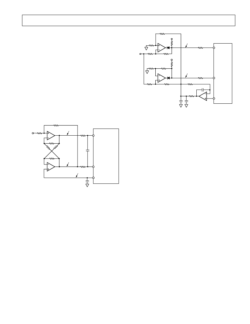
Figure 30 shows a cross-coupled differential driver circuit best
suited for systems in which the common-mode signal of the
input is already biased to approximately midsupply (i.e., 2.5 V).
The common-mode voltage of the differential output is set by
the voltage applied to the “+” input of A2. The closed loop
gain of this symmetrical driver can be easily set by R
IN
and R
F
.
For more insight into the operation of this cross-coupled driver,
please refer to the AD8042 data sheet.
VINA
VINB
CML
AD9243
0.1
m
F
1k
V
1k
V
1k
V
1k
V
R
IN
1k
V
V
IN
V
CML
–VIN
AV
DD
/2
V
CML
+VIN
AD8042
AD8042
33
V
33
V
C
F
*
*OPTIONAL NOISE/BAND LIMITING CAPACITOR
R
F
1k
V
Figure 30. Cross-Coupled Differential Driver
The driver circuit shown in Figure 31 is best suited for systems
in which the bipolar input signal is referenced to AGND and
requires proper level shifting. This driver circuit provides the
ability to level-shift the input signal to within the common-
mode range of the AD9243. The two op amps are configured as
matched difference amplifiers with the input signal applied to
opposing inputs to provide the differential output. The common-
mode offset voltage is applied to the noninverting resistor net-
work which provides the proper level shifting. The circuit also
employs optional diodes and pull-up resistors which may help
improve the op amps’ distortion performance by reducing their
headroom requirements. Rail-to-rail output amplifiers like the
AD8042 have sufficient headroom and thus do not require
these optional components.
VINA
VINB
CML
AD9243
390
V
390
V
V
IN
V
CML
–VIN
V
CML
+VIN
AV
DD
390
V
390
V
390
V
390
V
AV
DD
390
V
390
V
390
V
AD8047
AD8047
2.5k
V
33
V
100
V
0.1
m
F
1
m
F
0.1
m
F
OP113
33
V
390
V
Figure 31. Differential Driver with Level-Shifting
SINGLE-ENDED MODE OF OPERATION
The AD9243 can be configured for single-ended operation
using dc or ac coupling. In either case, the input of the A/D
must be driven from an operational amplifier that will not de-
grade the A/D’s performance. Because the A/D operates from a
single supply, it will be necessary to level shift ground-based
bipolar signals to comply with its input requirements. Both dc
and ac coupling provide this necessary function, but each
method results in different interface issues which may influence
the system design and performance.
DC COUPLING AND INTERFACE ISSUES
Many applications require the analog input signal to be dc
coupled to the AD9243. An operational amplifier can be con-
figured to rescale and level shift the input signal so that it is
compatible with the selected input range of the A/D. The input
range to the A/D should be selected on the basis of system
performance objectives as well as the analog power supply
availability since this will place certain constraints on the op
amp selection.
Many of the new high performance op amps are specified for
only
±
5 V operation and have limited input/output swing capa-
bilities. Hence, the selected input range of the AD9243 should
be sensitive to the headroom requirements of the particular op
amp to prevent clipping of the signal. Also, since the output of
a dual supply amplifier can swing below –0.3 V, clamping its
output should be considered in some applications.
In some applications, it may be advantageous to use an op amp
specified for single supply +5 V operation since it will inher-
ently limit its output swing to within the power supply rails.
Rail-to-rail output amplifiers such as the AD8041 allow the
AD9243 to be configured with larger input spans which im-
proves the noise performance.
相關PDF資料 |
PDF描述 |
|---|---|
| AD9243EB | Complete 14-Bit, 3.0 MSPS Monolithic A/D Converter |
| AD9243* | 14-Bit Rail-to-Rail DACs with I2C Interface; Package: DFN; No of Pins: 10; Temperature Range: 0°C to +70°C |
| AD9244 | 14-Bit, 40/65 MSPS Monolithic A/D Converter |
| AD9244-40PCB | 14-Bit, 40/65 MSPS Monolithic A/D Converter |
| AD9244-65PCB | 14-Bit, 40/65 MSPS Monolithic A/D Converter |
相關代理商/技術參數 |
參數描述 |
|---|---|
| AD9243ASRL | 制造商:Analog Devices 功能描述:ADC Single Pipelined 3Msps 14-bit Parallel 44-Pin MQFP T/R |
| AD9243ASZ | 功能描述:IC ADC 14BIT 3MSPS 44-MQFP RoHS:是 類別:集成電路 (IC) >> 數據采集 - 模數轉換器 系列:- 標準包裝:1 系列:microPOWER™ 位數:8 采樣率(每秒):1M 數據接口:串行,SPI? 轉換器數目:1 功率耗散(最大):- 電壓電源:模擬和數字 工作溫度:-40°C ~ 125°C 安裝類型:表面貼裝 封裝/外殼:24-VFQFN 裸露焊盤 供應商設備封裝:24-VQFN 裸露焊盤(4x4) 包裝:Digi-Reel® 輸入數目和類型:8 個單端,單極 產品目錄頁面:892 (CN2011-ZH PDF) 其它名稱:296-25851-6 |
| AD9243ASZRL | 功能描述:IC ADC 14BIT SGL 3MSPS 44MQFP RoHS:是 類別:集成電路 (IC) >> 數據采集 - 模數轉換器 系列:- 標準包裝:1,000 系列:- 位數:12 采樣率(每秒):300k 數據接口:并聯 轉換器數目:1 功率耗散(最大):75mW 電壓電源:單電源 工作溫度:0°C ~ 70°C 安裝類型:表面貼裝 封裝/外殼:24-SOIC(0.295",7.50mm 寬) 供應商設備封裝:24-SOIC 包裝:帶卷 (TR) 輸入數目和類型:1 個單端,單極;1 個單端,雙極 |
| AD9243EB | 制造商:AD 制造商全稱:Analog Devices 功能描述:Complete 14-Bit, 3.0 MSPS Monolithic A/D Converter |
| AD9243-EB | 制造商:Analog Devices 功能描述:Evaluation Board For AD9243 制造商:Analog Devices 功能描述:DEV TOOLS, EVAL BD FOR AD9243 - Bulk |
發布緊急采購,3分鐘左右您將得到回復。