- 您現在的位置:買賣IC網 > PDF目錄373962 > AD9244BST-65 (ANALOG DEVICES INC) 14-Bit, 40/65 MSPS Monolithic A/D Converter PDF資料下載
參數資料
| 型號: | AD9244BST-65 |
| 廠商: | ANALOG DEVICES INC |
| 元件分類: | ADC |
| 英文描述: | 14-Bit, 40/65 MSPS Monolithic A/D Converter |
| 中文描述: | 1-CH 14-BIT FLASH METHOD ADC, PARALLEL ACCESS, PQFP48 |
| 封裝: | MS-026-BBC, LQFP-48 |
| 文件頁數: | 18/36頁 |
| 文件大小: | 1845K |
| 代理商: | AD9244BST-65 |
第1頁第2頁第3頁第4頁第5頁第6頁第7頁第8頁第9頁第10頁第11頁第12頁第13頁第14頁第15頁第16頁第17頁當前第18頁第19頁第20頁第21頁第22頁第23頁第24頁第25頁第26頁第27頁第28頁第29頁第30頁第31頁第32頁第33頁第34頁第35頁第36頁
REV. A
–18–
AD9244
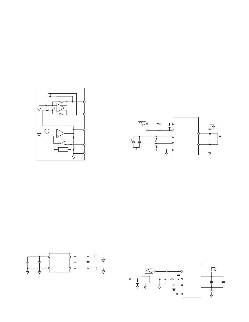
REFERENCE OPERATION
The AD9244 contains a band gap reference that provides a pin-
strappable option to generate either a 1 V or 2 V output. With the
addition of two external resistors, the user can generate reference
voltages between 1 V and 2 V. Another alternative is to use an
external reference for designs requiring enhanced accuracy and/or
drift performance as described later in this section. Figure 9a
shows a simplified model of the internal voltage reference of the
AD9244. A reference amplifier buffers a 1 V fixed reference. The
output from the reference amplifier, A1, appears on the VREF pin.
As stated earlier, the voltage on the VREF pin determines the
full-scale differential input span of the ADC.
REFT
REFB
VREF
SENSE
REFGND
AD9244
TO
ADC
2.5V
A1
A2
1V
LOGIC
DISABLE
A1
R
R
Figure 9a. Equivalent Reference Circuit
The voltage appearing at the VREF pin and the state of the internal
reference amplifier, A1, are determined by the voltage present at
the SENSE pin. The logic circuitry contains comparators that
monitor the voltage at the SENSE pin. The various reference
modes are summarized in Table II and are described in the next
few sections.
The actual reference voltages used by the internal circuitry of the
AD9244 appear on the REFT and REFB pins. The voltages on
these pins are symmetrical about midsupply or CML. For proper
operation, it is necessary to add a capacitor network to decouple
these pins. Figure 9b shows the recommended decoupling network.
The turn-on time of the reference voltage appearing between
REFT and REFB is approximately 10 ms and should be taken
into consideration in any power-down mode of operation. The
VREF pin should be bypassed to the REFGND pin with a 10
μ
F
tantalum capacitor in parallel with a low inductance 0.1
μ
F
ceramic capacitor.
10 F
0.1 F
0.1 F
0.1 F
0.1 F
*
10 F
VREF
REFT
REFB
AD9244
*
LOCATE AS CLOSE AS POSSIBLE TO REFT/REFB PINS
REFGND
+
+
Figure 9b. Reference Decoupling
Pin Programmable Reference
By shorting the VREF pin directly to the SENSE pin, the internal
reference amplifier is placed in a unity gain mode and the resulting
VREF output is 1 V. By shorting the SENSE pin directly to the
REFGND pin, the internal reference amplifier is configured for a
gain of 2.0 and the resulting VREF output is 2.0 V.
Resistor Programmable Reference
Figure 10 shows an example of how to generate a reference voltage
other than 1.0 V or 2.0 V with the addition of two external
resistors. Use the equation
VREF
V
R R
/
=
×
+
(
)
1
1
to determine the appropriate values for
R
1 and
R
2. These resistors
should be in the 2 k
to 10 k
range. For the example shown,
R
1 equals 2.5 k
and
R
2 equals 5 k
. From the equation above,
the resulting reference voltage on the VREF pin is 1.5 V. This
sets the differential input span to 1.5 V p-p. The midscale voltage
can also be set to VREF by connecting VIN
–
to VREF.
10 F
0.1 F
10 F
0.1 F
0.1 F
0.1 F
REFT
REFB
VREF
SENSE
REFGND
AD9244
VIN+
VIN–
3.25V
1.75V
2.5V
1.5V
33
33
20pF
R1
2.5k
R2
5k
Figure 10. Resistor Programmable Reference (1.5 V p-p
Input Span, Differential Input with VCM = 2.5 V)
Using an External Reference
To use an external reference, the internal reference must be
disabled by connecting the SENSE pin to AVDD. The AD9244
contains an internal reference buffer, A2 (see Figure 9a), that
simplifies the drive requirements of an external reference. The
external reference must be able to drive a 5 k
(
±
20%) load. The
bandwidth of the reference is deliberately left small to minimize
the reference noise contribution. As a result, it is not possible to
drive VREF externally with high frequencies.
Figure 11 shows an example of an external reference driving both
VIN
–
and VREF. In this case, both the common-mode voltage
and input span are directly dependent on the value of VREF.
Both the input span and the center of the input span are equal
to the external VREF. Thus the valid input range extends from
(VREF
+ VREF/2) to (VREF
–
VREF/2). For example, if the
precision reference part, REF191, a 2.048 V external reference,
is used, the input span is 2.048 V. In this case, 1 LSB of the
AD9244 corresponds to 0.125 mV. It is essential that a minimum
of a 10
μ
F capacitor, in parallel with a 0.1
μ
F low inductance
ceramic capacitor, decouple the reference output to AGND.
VIN+
VREF
VIN–
SENSE
20pF
VREF + VREF/2
33
33
REFT
REFB
VREF – VREF/2
VREF
0.1 F
5V
AVDD
0.1 F
0.1 F
0.1 F
0.1 F
10 F
+
10 F
AD9244
Figure 11. Using an External Reference
相關PDF資料 |
PDF描述 |
|---|---|
| AD9244BST-40 | 14-Bit, 40/65 MSPS Monolithic A/D Converter |
| AD9245 | 14-Bit, 80 MSPS, 3 V A/D Converter |
| AD9245BCP-80 | 14-Bit, 80 MSPS, 3 V A/D Converter |
| AD9245BCPRL7-80 | 14-Bit, 80 MSPS, 3 V A/D Converter |
| AD9245BCPZ-80 | 14-Bit, 80 MSPS, 3 V A/D Converter |
相關代理商/技術參數 |
參數描述 |
|---|---|
| AD9244BSTRL-40 | 制造商:AD 制造商全稱:Analog Devices 功能描述:14-Bit, 40/65 MSPS Monolithic A/D Converter |
| AD9244BSTRL-65 | 制造商:Analog Devices 功能描述:Single ADC Pipelined 65Msps 14-bit Parallel 48-Pin LQFP T/R |
| AD9244BSTZ40 | 制造商:Analog Devices 功能描述: |
| AD9244BSTZ-40 | 功能描述:IC ADC 14BIT 40MSPS 48-LQFP RoHS:是 類別:集成電路 (IC) >> 數據采集 - 模數轉換器 系列:- 標準包裝:1 系列:microPOWER™ 位數:8 采樣率(每秒):1M 數據接口:串行,SPI? 轉換器數目:1 功率耗散(最大):- 電壓電源:模擬和數字 工作溫度:-40°C ~ 125°C 安裝類型:表面貼裝 封裝/外殼:24-VFQFN 裸露焊盤 供應商設備封裝:24-VQFN 裸露焊盤(4x4) 包裝:Digi-Reel® 輸入數目和類型:8 個單端,單極 產品目錄頁面:892 (CN2011-ZH PDF) 其它名稱:296-25851-6 |
| AD9244BSTZ-401 | 制造商:AD 制造商全稱:Analog Devices 功能描述:14-Bit, 40 MSPS/65 MSPS A/D Converter |
發布緊急采購,3分鐘左右您將得到回復。