- 您現(xiàn)在的位置:買賣IC網(wǎng) > PDF目錄4590 > AD9267BCPZRL7 (Analog Devices Inc)IC MOD SIGMA-DELTA DUAL 64LFCSP PDF資料下載
參數(shù)資料
| 型號: | AD9267BCPZRL7 |
| 廠商: | Analog Devices Inc |
| 文件頁數(shù): | 1/24頁 |
| 文件大小: | 0K |
| 描述: | IC MOD SIGMA-DELTA DUAL 64LFCSP |
| 標準包裝: | 750 |
| 類型: | 三角積分調(diào)制器 |
| 應(yīng)用: | 無線通信系統(tǒng) |
| 安裝類型: | 表面貼裝 |
| 封裝/外殼: | 64-VFQFN 裸露焊盤,CSP |
| 供應(yīng)商設(shè)備封裝: | 64-LFCSP-VQ(9x9) |
| 包裝: | 帶卷 (TR) |
10 MHz Bandwidth, 640 MSPS
Dual Continuous Time Sigma-Delta Modulator
AD9267
Rev. 0
Information furnished by Analog Devices is believed to be accurate and reliable. However, no
responsibilityis assumedbyAnalogDevicesforitsuse,norforanyinfringementsof patentsorother
rightsofthirdpartiesthatmayresultfromitsuse.Specificationssubjecttochangewithoutnotice.No
license is granted by implication or otherwise under any patent or patent rights of Analog Devices.
Trademarksandregisteredtrademarksarethepropertyoftheirrespectiveowners.
One Technology Way, P.O. Box 9106, Norwood, MA 02062-9106, U.S.A.
Tel: 781.329.4700
Fax: 781.461.3113
2009 Analog Devices, Inc. All rights reserved.
FEATURES
SNR: 83 dB (85 dBFS) to 10 MHz input
SFDR: 88 dBc to 10 MHz input
Noise figure: 15 dB
Input impedance: 1 kΩ
Power: 416 mW
10 MHz real or 20 MHz complex bandwidth
1.8 V analog supply operation
On-chip PLL clock multiplier
On-chip voltage reference
Twos complement data format
640 MSPS, 4-bit LVDS data output
Serial control interface (SPI)
APPLICATIONS
Baseband quadrature receivers: CDMA2000, W-CDMA,
multicarrier GSM/EDGE, 802.16x, and LTE
Quadrature sampling instrumentation
GENERAL DESCRIPTION
The AD9267 is a dual continuous time (CT) sigma-delta (Σ-Δ)
modulator with 88 dBc of dynamic range over 10 MHz real
or 20 MHz complex bandwidth. The combination of high
dynamic range, wide bandwidth, and characteristics unique
to the continuous time Σ-Δ modulator architecture makes the
AD9267 an ideal solution for wireless communication systems.
The AD9267 has a resistive input impedance that significantly
relaxes the requirements of the driver amplifier. In addition, a
32× oversampled fifth-order continuous time loop filter attenuates
out-of-band signals and aliases, reducing the need for external
filters at the input. The low noise figure of 15 dB relaxes the
linearity requirements of the front-end signal chain components,
and the high dynamic range reduces the need for an automatic
gain control (AGC) loop.
A differential input clock controls all internal conversion cycles.
An external clock input or the integrated integer-N PLL provides
the 640 MHz internal clock needed for the oversampled conti-
nuous time Σ-Δ modulator. The digital output data is presented
as 4-bit, LVDS at 640 MSPS in twos complement format. A data
clock output (DCO) is provided to ensure proper latch timing
with receiving logic. Additional digital signal processing may be
required on the 4-bit modulator output to remove the out-of-band
noise and to reduce the sample rate.
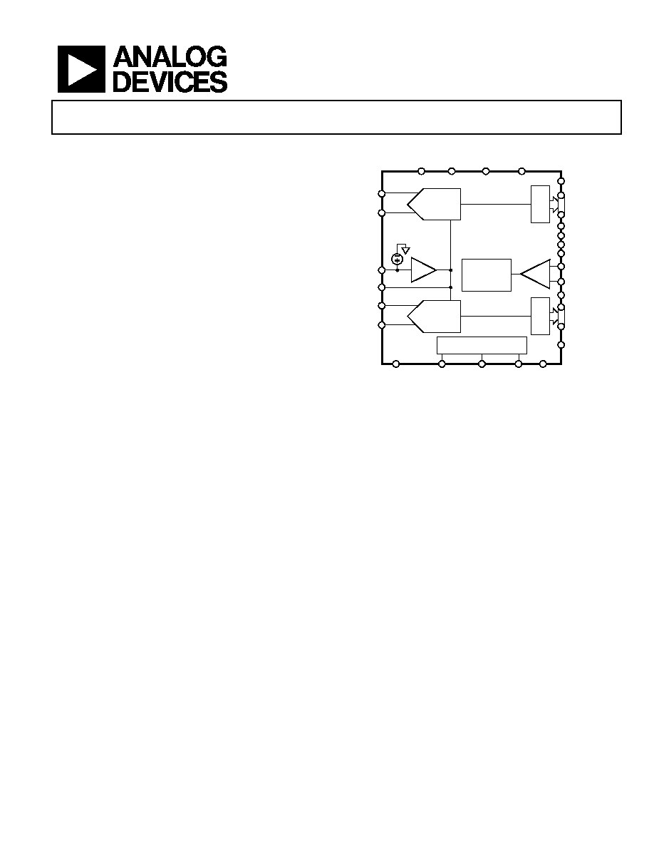
FUNCTIONAL BLOCK DIAGRAM
VIN+A
VIN–A
VIN+B
VIN–B
VREF
CFILT
07
77
3-
00
1
PHASE-
LOCKED
LOOP
SERIAL
INTERFACE
LV
D
S
DRI
V
E
RS
LV
D
S
DR
IV
E
RS
Σ-Δ
MODULATOR
Σ-Δ
MODULATOR
AGND
SDIO/
PLLMULT1
SCLK/
PLLMULT0
DGND
CSB
AVDD
PDWNB
PDWNA
DRVDD
AD9267
D3±A
OR±A
D0±A
D3±B
D0±B
CLK+
PLLMULT2
PLLMULT3
PLLMULT4
PLL_LOCKED
CLK–
DCO±
OR±B
Figure 1.
The AD9267 operates on a 1.8 V power supply, consuming
416 mW. The AD9267 is available in a 64-lead LFCSP and
is specified over the industrial temperature range (40°C
to +85°C).
PRODUCT HIGHLIGHTS
1.
Continuous time Σ-Δ architecture efficiently achieves high
dynamic range and wide bandwidth.
2.
Passive input structure reduces or eliminates the require-
ments for a driver amplifier.
3.
An oversampling ratio of 32× and high order loop filter
provide excellent alias rejection, reducing or eliminating
the need for antialiasing filters.
4.
Operates from a single 1.8 V power supply.
5.
A standard serial port interface (SPI) supports various
product features and functions.
6.
Features a low pin count, high speed LVDS interface with
data output clock.
相關(guān)PDF資料 |
PDF描述 |
|---|---|
| LFXP6E-4F256C | IC FPGA 5.8KLUTS 188I/O 256-BGA |
| LFXP6E-3F256I | IC FPGA 5.8KLUTS 188I/O 256-BGA |
| HBC65DRYI | CONN EDGECARD 130PS DIP .100 SLD |
| LFXP6E-4FN256C | IC FPGA 5.8KLUTS 256FPBGA |
| LFXP6E-3FN256I | IC FPGA 5.8KLUTS 188I/O 256-BGA |
相關(guān)代理商/技術(shù)參數(shù) |
參數(shù)描述 |
|---|---|
| AD9267EBZ | 功能描述:BOARD EVALUATION FOR AD9267 RoHS:是 類別:編程器,開發(fā)系統(tǒng) >> 評估板 - 模數(shù)轉(zhuǎn)換器 (ADC) 系列:- 產(chǎn)品培訓(xùn)模塊:Obsolescence Mitigation Program 標準包裝:1 系列:- ADC 的數(shù)量:1 位數(shù):12 采樣率(每秒):94.4k 數(shù)據(jù)接口:USB 輸入范圍:±VREF/2 在以下條件下的電源(標準):- 工作溫度:-40°C ~ 85°C 已用 IC / 零件:MAX11645 已供物品:板,軟件 |
| AD9268 | 制造商:AD 制造商全稱:Analog Devices 功能描述:16-Bit, 80 MSPS/105 MSPS/125 MSPS, 1.8 V Dual Analog-to-Digital Converter (ADC) |
| AD9268-105EBZ1 | 制造商:AD 制造商全稱:Analog Devices 功能描述:16-Bit, 80 MSPS/105 MSPS/125 MSPS, 1.8 V Dual Analog-to-Digital Converter (ADC) |
| AD9268-125EBZ | 功能描述:數(shù)據(jù)轉(zhuǎn)換 IC 開發(fā)工具 Dual 16 bit 125 high SNR ADC RoHS:否 制造商:Texas Instruments 產(chǎn)品:Demonstration Kits 類型:ADC 工具用于評估:ADS130E08 接口類型:SPI 工作電源電壓:- 6 V to + 6 V |
| AD9268-125EBZ1 | 制造商:AD 制造商全稱:Analog Devices 功能描述:16-Bit, 80 MSPS/105 MSPS/125 MSPS, 1.8 V Dual Analog-to-Digital Converter (ADC) |
發(fā)布緊急采購,3分鐘左右您將得到回復(fù)。