- 您現在的位置:買賣IC網 > PDF目錄17022 > AD9279-65EBZ (Analog Devices Inc)BOARD EVALUATION FOR AD9279 PDF資料下載
參數資料
| 型號: | AD9279-65EBZ |
| 廠商: | Analog Devices Inc |
| 文件頁數: | 1/44頁 |
| 文件大小: | 0K |
| 描述: | BOARD EVALUATION FOR AD9279 |
| 標準包裝: | 1 |
| ADC 的數量: | 8 |
| 位數: | 12 |
| 采樣率(每秒): | 80M |
| 數據接口: | 串行 |
| 工作溫度: | -40°C ~ 85°C |
| 已用 IC / 零件: | AD9279 |
| 已供物品: | 板 |
當前第1頁第2頁第3頁第4頁第5頁第6頁第7頁第8頁第9頁第10頁第11頁第12頁第13頁第14頁第15頁第16頁第17頁第18頁第19頁第20頁第21頁第22頁第23頁第24頁第25頁第26頁第27頁第28頁第29頁第30頁第31頁第32頁第33頁第34頁第35頁第36頁第37頁第38頁第39頁第40頁第41頁第42頁第43頁第44頁
Octal LNA/VGA/AAF/ADC
and CW I/Q Demodulator
AD9279
Rev. 0
Information furnished by Analog Devices is believed to be accurate and reliable. However, no
responsibilityis assumedbyAnalogDevicesforitsuse,norforanyinfringements of patents or other
rightsofthirdpartiesthatmayresultfromitsuse.Specificationssubjecttochangewithoutnotice.No
license is granted by implication or otherwise under any patent or patent rights of Analog Devices.
Trademarksandregisteredtrademarksarethepropertyoftheirrespectiveowners.
One Technology Way, P.O. Box 9106, Norwood, MA 02062-9106, U.S.A.
Tel: 781.329.4700
www.analog.com
Fax: 781.461.3113
2010 Analog Devices, Inc. All rights reserved.
FEATURES
8 channels of LNA, VGA, AAF, ADC, and I/Q demodulator
Low power: 141 mW per channel, TGC mode, 40 MSPS;
60 mW per channel, CW mode
10 mm × 10 mm, 144-ball CSP-BGA
TGC channel input-referred noise: 0.8 nV/
√Hz, max gain
Flexible power-down modes
Fast recovery from low power standby mode: <2 μs
Overload recovery: <10 ns
Low noise preamplifier (LNA)
Input-referred noise: 0.75 nV/√Hz, gain = 21.3 dB
Programmable gain: 15.6 dB/17.9 dB/21.3 dB
0.1 dB compression: 1000 mV p-p/
750 mV p-p/450 mV p-p
Dual-mode active input impedance matching
Bandwidth (BW): >100 MHz
Variable gain amplifier (VGA)
Attenuator range: 45 dB to 0 dB
Postamp gain (PGA): 21 dB/24 dB/27 dB/30 dB
Linear-in-dB gain control
Antialiasing filter (AAF)
Programmable second-order LPF from 8 MHz to 18 MHz
Programmable HPF
Analog-to-digital converter (ADC)
SNR: 70 dB, 12 bits up to 80 MSPS
Serial LVDS (ANSI-644, low power/reduced signal)
CW mode I/Q demodulator
Individual programmable phase rotation
Output dynamic range per channel: >160 dBc/√Hz
Output-referred SNR: 155 dBc/√Hz, 1 kHz offset, 3 dBFS
GENERAL DESCRIPTION
The AD9279 is designed for low cost, low power, small size,
and ease of use for medical ultrasound and automotive radar. It
contains eight channels of a variable gain amplifier (VGA) with
a low noise preamplifier (LNA), an antialiasing filter (AAF), an
analog-to-digital converter (ADC), and an I/Q demodulator
with programmable phase rotation.
Each channel features a variable gain range of 45 dB, a fully
differential signal path, an active input preamplifier termination,
and a maximum gain of up to 52 dB. The channel is optimized
for high dynamic performance and low power in applications
where a small package size is critical.
The LNA has a single-ended-to-differential gain that is selectable
through the SPI. Assuming a 15 MHz noise bandwidth (NBW)
and a 21.3 dB LNA gain, the LNA input SNR is roughly 94 dB.
In CW Doppler mode, each LNA output drives an I/Q demod-
ulator that has independently programmable phase rotation
with 16 phase settings.
Power-down of individual channels is supported to increase
battery life for portable applications. Standby mode allows quick
power-up for power cycling. In CW Doppler operation, the
VGA, AAF, and ADC are powered down. The ADC contains
several features designed to maximize flexibility and minimize
system cost, such as a programmable clock, data alignment, and
programmable digital test pattern generation. The digital test
patterns include built-in fixed patterns, built-in pseudo random
patterns, and custom user-defined test patterns entered via the
serial port interface.
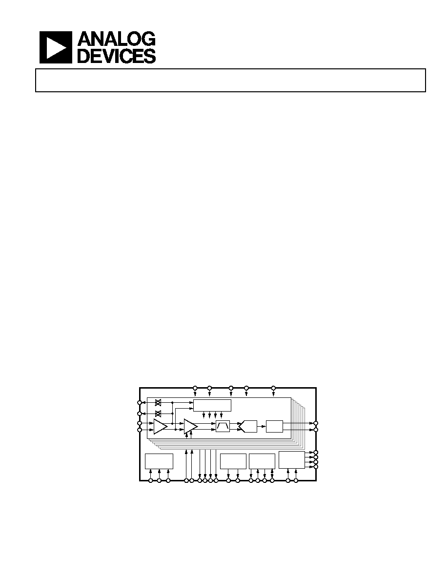
FUNCTIONAL BLOCK DIAGRAM
094
23-
0
01
AAF
12-BIT
ADC
VGA
LNA
SERIAL
LVDS
I/Q
DEMODULATOR
8 CHANNELS
SERIAL
PORT
INTERFACE
DATA
RATE
MULTIPLIER
REFERENCE
LO
GENERATION
LO-A TO LO-H
LOSW-A TO LOSW-H
LI-A TO LI-H
LG-A TO LG-H
DOUTA+ TO DOUTH+
DOUTA– TO DOUTH–
FCO+
DRVDD
CL
K–
CLK+
SD
IO
SC
L
K
CS
B
GP
O[0
:3
]
RB
IAS
VR
EF
CW
Q
+
CW
Q
–
CW
I+
CW
I–
GA
IN
–
GA
IN
+
4L
O
–
4L
O
+
RE
S
E
T
STBY
PDWN
AVDD2
AVDD1
FCO–
DCO+
DCO–
Figure 1.
相關PDF資料 |
PDF描述 |
|---|---|
| AD9222-65EBZ | BOARD EVALUATION AD9222 65MSPS |
| CM453232-102KL | INDUCTR CHIP 1000UH 10% 1812 SMD |
| 1210R-681K | COIL .68UH IRON SMD |
| AD9212-65EBZ | BOARD EVALUATION FOR AD9212 |
| MAX11040EVKIT+ | KIT EVALUATION FOR MAX11040 |
相關代理商/技術參數 |
參數描述 |
|---|---|
| AD9279-80KITZ | 功能描述:KIT EVALUATION FOR AD9279 RoHS:是 類別:編程器,開發系統 >> 評估板 - 模數轉換器 (ADC) 系列:- 產品培訓模塊:Obsolescence Mitigation Program 標準包裝:1 系列:- ADC 的數量:1 位數:12 采樣率(每秒):94.4k 數據接口:USB 輸入范圍:±VREF/2 在以下條件下的電源(標準):- 工作溫度:-40°C ~ 85°C 已用 IC / 零件:MAX11645 已供物品:板,軟件 |
| AD9279BBCZ | 功能描述:IC ADC 12BIT 80MSPS 144CSPBGA RoHS:是 類別:集成電路 (IC) >> 數據采集 - ADCs/DAC - 專用型 系列:- 產品培訓模塊:Lead (SnPb) Finish for COTS Obsolescence Mitigation Program 標準包裝:50 系列:- 類型:數據采集系統(DAS) 分辨率(位):16 b 采樣率(每秒):21.94k 數據接口:MICROWIRE?,QSPI?,串行,SPI? 電壓電源:模擬和數字 電源電壓:1.8 V ~ 3.6 V 工作溫度:-40°C ~ 85°C 安裝類型:表面貼裝 封裝/外殼:40-WFQFN 裸露焊盤 供應商設備封裝:40-TQFN-EP(6x6) 包裝:托盤 |
| AD9279-BBCZ | 制造商:AD 制造商全稱:Analog Devices 功能描述:Octal LNA/VGA/AAF/ADC and CW I/Q Demodulator |
| AD9280 | 制造商:AD 制造商全稱:Analog Devices 功能描述:Complete 8-Bit, 32 MSPS, 95 mW CMOS A/D Converter |
| AD9280ARS | 功能描述:IC ADC CMOS 8BIT 32MSPS 28-SSOP RoHS:否 類別:集成電路 (IC) >> 數據采集 - 模數轉換器 系列:- 產品培訓模塊:Lead (SnPb) Finish for COTS Obsolescence Mitigation Program 標準包裝:2,500 系列:- 位數:12 采樣率(每秒):3M 數據接口:- 轉換器數目:- 功率耗散(最大):- 電壓電源:- 工作溫度:- 安裝類型:表面貼裝 封裝/外殼:SOT-23-6 供應商設備封裝:SOT-23-6 包裝:帶卷 (TR) 輸入數目和類型:- |
發布緊急采購,3分鐘左右您將得到回復。