- 您現在的位置:買賣IC網 > PDF目錄373962 > AD9280ARSRL (ANALOG DEVICES INC) Complete 8-Bit, 32 MSPS, 95 mW CMOS A/D Converter PDF資料下載
參數資料
| 型號: | AD9280ARSRL |
| 廠商: | ANALOG DEVICES INC |
| 元件分類: | ADC |
| 英文描述: | Complete 8-Bit, 32 MSPS, 95 mW CMOS A/D Converter |
| 中文描述: | 1-CH 8-BIT PROPRIETARY METHOD ADC, PARALLEL ACCESS, PDSO28 |
| 封裝: | SSOP-28 |
| 文件頁數: | 14/24頁 |
| 文件大小: | 366K |
| 代理商: | AD9280ARSRL |
AD9280
–14–
REV. D
DRIVING THE ANALOG INPUT
Figure 25 shows the equivalent analog input of the AD9280, a
sample-and-hold amplifier (switched capacitor input SHA).
Bringing CLK to a logic low level closes Switches 1 and 2 and
opens Switch 3. The input source connected to AIN must
charge capacitor CH during this time. When CLK transitions
from logic “low” to logic “high,” Switches 1 and 2 open, placing
the SHA in hold mode. Switch 3 then closes, forcing the output
of the op amp to equal the voltage stored on CH. When CLK
transitions from logic “high” to logic “low,” Switch 3 opens
first. Switches 1 and 2 close, placing the SHA in track mode.
The structure of the input SHA places certain requirements on
the input drive source. The combination of the pin capacitance,
CP, and the hold capacitance, CH, is typically less than 5 pF.
The input source must be able to charge or discharge this ca-
pacitance to 8-bit accuracy in one half of a clock cycle. When
the SHA goes into track mode, the input source must charge or
discharge capacitor CH from the voltage already stored on CH
to the new voltage. In the worst case, a full-scale voltage step on
the input, the input source must provide the charging current
through the R
ON
(50
) of Switch 1 and quickly (within 1/2CLK
period) settle. This situation corresponds to driving a low input
impedance. On the other hand, when the source voltage equals
the value previously stored on CH, the hold capacitor requires
no input current and the equivalent input impedance is ex-
tremely high.
Adding series resistance between the output of the source and
the AIN pin reduces the drive requirements placed on the
source. Figure 26 shows this configuration. The bandwidth of
the particular application limits the size of this resistor. To
maintain the performance outlined in the data sheet specifica-
tions, the resistor should be limited to 20
or less. For applica-
tions with signal bandwidths less than 16 MHz, the user may
proportionally increase the size of the series resistor. Alterna-
tively, adding a shunt capacitance between the AIN pin and
analog ground can lower the ac load impedance. The value of
this capacitance will depend on the source resistance and the
required signal bandwidth.
The input span of the AD9280 is a function of the reference
voltages. For more information regarding the input range, see
the Internal and External Reference sections of the data sheet.
CH
CH
CP
CP
S1
S3
S2
AIN
(REFTS
REFBS)
SHA
AD9280
Figure 25. AD9280 Equivalent Input Structure
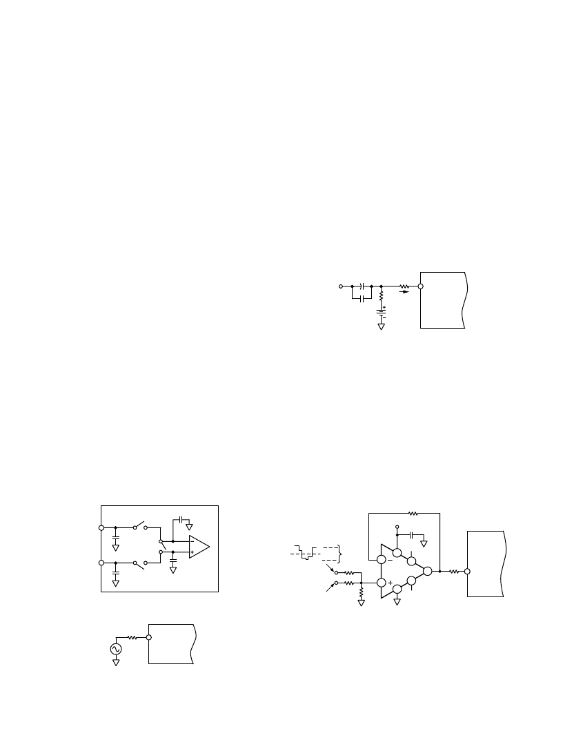
AIN
V
S
< 20
V
AD9280
Figure 26. Simple AD9280 Drive Configuration
In many cases, particularly in single-supply operation, ac cou-
pling offers a convenient way of biasing the analog input signal
at the proper signal range. Figure 27 shows a typical configura-
tion for ac-coupling the analog input signal to the AD9280.
Maintaining the specifications outlined in the data sheet
requires careful selection of the component values. The most
important is the f
–3 dB
high-pass corner frequency. It is a function of
R2 and the parallel combination of C1 and C2. The f
–3 dB
point
can be approximated by the equation:
f
–3 dB
= 1/(2
×
pi
×
[
R
2]
C
EQ
)
where
C
EQ
is the parallel combination of C1 and C2. Note that
C1 is typically a large electrolytic or tantalum capacitor that
becomes inductive at high frequencies. Adding a small ceramic
or polystyrene capacitor (on the order of 0.01
μ
F) that does not
become inductive until negligibly higher frequencies, maintains
a low impedance over a wide frequency range.
NOTE: AC coupled input signals may also be shifted to a desired
level with the AD9280’s internal clamp. See Clamp Operation.
AIN
R1
AD9280
I
B
R2
V
BIAS
C1
C2
V
IN
Figure 27. AC Coupled Input
There are additional considerations when choosing the resistor
values. The ac-coupling capacitors integrate the switching tran-
sients present at the input of the AD9280 and cause a net dc
bias current, I
B
, to flow into the input. The magnitude of the
bias current increases as the signal magnitude deviates from
V midscale and the clock frequency increases; i.e., minimum
bias current flow when AIN = V midscale. This bias current
will result in an offset error of (R1 + R2)
×
I
B
. If it is necessary
to compensate this error, consider making R2 negligibly small or
modifying VBIAS to account for the resultant offset.
In systems that must use dc coupling, use an op amp to level-
shift a ground-referenced signal to comply with the input re-
quirements of the AD9280. Figure 28 shows an AD8041 config-
ured in noninverting mode.
AIN
20
V
AD9280
6
7
2
3
4
NC
0.1
m
F
+V
CC
NC
MIDSCALE
OFFSET
VOLTAGE
0V
DC
1V p-p
AD8041
5
1
Figure 28. Bipolar Level Shift
相關PDF資料 |
PDF描述 |
|---|---|
| AD9280 | Complete 8-Bit, 32 MSPS, 95 mW CMOS A/D Converter |
| AD9280-EB | Complete 8-Bit, 32 MSPS, 95 mW CMOS A/D Converter |
| AD9280ARS | Complete 8-Bit, 32 MSPS, 95 mW CMOS A/D Converter |
| AD9281 | Dual Channel 8-Bit Resolution CMOS ADC |
| AD9281-EB | Dual Channel 8-Bit Resolution CMOS ADC |
相關代理商/技術參數 |
參數描述 |
|---|---|
| AD9280ARSZ | 功能描述:IC ADC CMOS 8BIT 32MSPS 28-SSOP RoHS:是 類別:集成電路 (IC) >> 數據采集 - 模數轉換器 系列:- 標準包裝:1 系列:microPOWER™ 位數:8 采樣率(每秒):1M 數據接口:串行,SPI? 轉換器數目:1 功率耗散(最大):- 電壓電源:模擬和數字 工作溫度:-40°C ~ 125°C 安裝類型:表面貼裝 封裝/外殼:24-VFQFN 裸露焊盤 供應商設備封裝:24-VQFN 裸露焊盤(4x4) 包裝:Digi-Reel® 輸入數目和類型:8 個單端,單極 產品目錄頁面:892 (CN2011-ZH PDF) 其它名稱:296-25851-6 |
| AD9280ARSZRL | 功能描述:IC ADC 8BIT CMOS 32MSPS 28SSOP RoHS:是 類別:集成電路 (IC) >> 數據采集 - 模數轉換器 系列:- 標準包裝:2,500 系列:- 位數:16 采樣率(每秒):15 數據接口:MICROWIRE?,串行,SPI? 轉換器數目:1 功率耗散(最大):480µW 電壓電源:單電源 工作溫度:-40°C ~ 85°C 安裝類型:表面貼裝 封裝/外殼:38-WFQFN 裸露焊盤 供應商設備封裝:38-QFN(5x7) 包裝:帶卷 (TR) 輸入數目和類型:16 個單端,雙極;8 個差分,雙極 配用:DC1011A-C-ND - BOARD DELTA SIGMA ADC LTC2494 |
| AD9280-EB | 制造商:Analog Devices 功能描述:EVAL BD FOR AD9280 - Bulk |
| AD9280JRS | 制造商:未知廠家 制造商全稱:未知廠家 功能描述:Analog-to-Digital Converter, 8-Bit |
| AD9280JRSRL | 制造商:未知廠家 制造商全稱:未知廠家 功能描述:Analog-to-Digital Converter, 8-Bit |
發布緊急采購,3分鐘左右您將得到回復。