- 您現在的位置:買賣IC網 > PDF目錄373962 > AD9430 (Analog Devices, Inc.) 12-Bit, 170 MSPS 3.3V A/D Converter PDF資料下載
參數資料
| 型號: | AD9430 |
| 廠商: | Analog Devices, Inc. |
| 英文描述: | 12-Bit, 170 MSPS 3.3V A/D Converter |
| 中文描述: | 12位,170 MSPS的3.3VA / D轉換器 |
| 文件頁數: | 13/20頁 |
| 文件大小: | 1594K |
| 代理商: | AD9430 |
PRELIMINARY TECHNICAL DATA
AD9430
REV. PrG 4/01/2002
-13-
Digital Outputs
The off chip drivers on the chip can be configured by the
user to provide CMOS or LVDS compatible output levels
via pin S2.
The CMOS digital outputs (
S2=0
) are TTL/CMOS-
compatible for lower power consumption. The outputs are
biased from a separate supply (VDD), allowing easy
interface to external logic. The outputs are CMOS devices
which will swing from ground to VDD (with no dc load). It
is recommended to minimize the capacitive load the ADC
drives by keeping the output traces short (<1 inch, for a total
C
LOAD
< 5 pF). When operating in cmos mode it is also
recommended to place low value (220 ohm) series damping
resistors on the data lines to reduce switching transient
effects on performance.
LVDS outputs are available when S2=VDD and a 3.7K
RSET resistor is placed at pin 7 (
LVDSBIAS
) to ground .
This resistor sets the output current at each output equal to a
nominal 3.5mA ( 10* I
RSET
) . A 100 ohm differential
termination resistor placed at the lvds receiver inputs results
in a nominal 350mV voltage swing at the receiver. Note that
when operating in LVDS mode the output supply must be at
a dc potential greater than or equal to the analog supply level
(AVDD). This can be accomplished simply by biasing the
two supplies from the same power plane or by tying the two
supplies on the pcb through an inductor. When operating in
CMOS mode this is not required and separate supplies are
recommended.
Clock Outputs (DCO+, DCO-)
The input ENCODE is divided by two (in CMOS mode) and
available off-chip at DCO+ and DCO-. These clocks can
facilitate latching off-chip, providing a low skew clocking
solution (see timing diagram). The on-chip clock buffers
should not drive more than 5 pF of capacitance to limit
switching transient effects on performance.
Note that the Outputs clocks are CMOS levels when CMOS
mode is selected(S2=0) and are LVDS levels when in LVDS
mode(S2=VDD). (Requiring a 100ohm differential
termination at receiver in LVDS mode). The output clock in
LVDS mode switches at the encode rate.
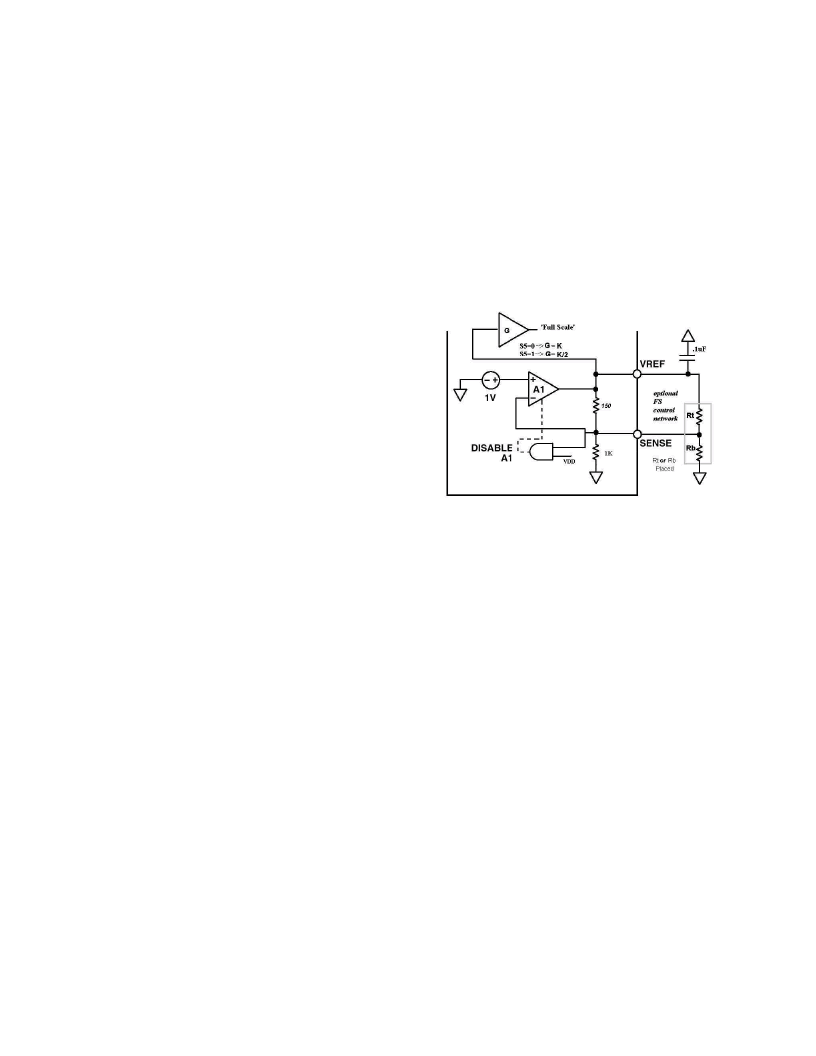
Voltage Reference
A stable and accurate 1.25 V voltage reference is built into
the AD9430 (VREF). The analog input Full Scale Range is
linearly proportional to the voltage at VREF. VREF (
and in
turn input full scale
) can be varied by adding an external
resistor network at VREF, SENSE and GROUND. (See
figure X ) . No appreciable degradation in performance
occurs when VREF is adjusted ±5%. Note that an external
reference can be used by connecting the SENSE pin to VDD
(disabling internal reference) and driving VREF with the
external reference source. A .1uF capacitor to ground is
recommended at VREF pin in internal and external reference
applications.
Simplified Voltage Reference Equivalent Circuit
相關PDF資料 |
PDF描述 |
|---|---|
| AD9430BSV-170 | 12-Bit, 170 MSPS 3.3V A/D Converter |
| AD9432BST-80 | 12-Bit, 80 MSPS/105 MSPS A/D Converter |
| AD9432BST-105 | 12-Bit, 80 MSPS/105 MSPS A/D Converter |
| AD9432BSQ-105 | 12-Bit, 80 MSPS/105 MSPS A/D Converter |
| AD9432BSQ-80 | 12-Bit, 80 MSPS/105 MSPS A/D Converter |
相關代理商/技術參數 |
參數描述 |
|---|---|
| AD9430/PCB-CMOS | 制造商:AD 制造商全稱:Analog Devices 功能描述:12-Bit, 170 MSPS 3.3V A/D Converter |
| AD9430_10 | 制造商:AD 制造商全稱:Analog Devices 功能描述:12-Bit, 170/210 MSPS 3.3 V A/D Converter |
| AD9430BSV-170 | 制造商:Analog Devices 功能描述:ADC Single Pipelined 170Msps 12-bit Parallel 100-Pin TQFP EP 制造商:Rochester Electronics LLC 功能描述:- Bulk 制造商:Analog Devices 功能描述:IC 12-BIT ADC |
| AD9430BSV-210 | 制造商:Analog Devices 功能描述:ADC Single Pipelined 210Msps 12-bit Parallel 100-Pin TQFP EP 制造商:Analog Devices 功能描述:IC ADC 12BIT 210MSPS TQFP-100 |
| AD9430BSV-270 | 制造商:Analog Devices 功能描述:12 BIT 170 MSPS ADC - Bulk |
發布緊急采購,3分鐘左右您將得到回復。