- 您現在的位置:買賣IC網 > PDF目錄373963 > AD9445-IF-LVDS (Analog Devices, Inc.) 14-Bit, 105/125 MSPS, IF Sampling ADC PDF資料下載
參數資料
| 型號: | AD9445-IF-LVDS |
| 廠商: | Analog Devices, Inc. |
| 英文描述: | 14-Bit, 105/125 MSPS, IF Sampling ADC |
| 中文描述: | 14位,一百二十五分之一百○五MSPS的,中頻采樣ADC |
| 文件頁數: | 25/40頁 |
| 文件大小: | 965K |
| 代理商: | AD9445-IF-LVDS |
第1頁第2頁第3頁第4頁第5頁第6頁第7頁第8頁第9頁第10頁第11頁第12頁第13頁第14頁第15頁第16頁第17頁第18頁第19頁第20頁第21頁第22頁第23頁第24頁當前第25頁第26頁第27頁第28頁第29頁第30頁第31頁第32頁第33頁第34頁第35頁第36頁第37頁第38頁第39頁第40頁

AD9445
External Reference Operation
The AD9445’s internal reference is trimmed to enhance the gain
accuracy of the ADC. An external reference may be more stable
over temperature, but the gain of the ADC is not likely to improve.
Figure 49 shows the typical drift characteristics of the internal
reference in both 1 V and 0.5 V modes.
Rev. 0 | Page 25 of 40
3.5V
VIN+
VIN–
1V p-p
DIGITAL OUT = ALL 1s
DIGITAL OUT = ALL 0s
0
When the SENSE pin is tied to AVDD, the internal reference is
disabled, allowing the use of an external reference. An internal
reference buffer loads the external reference with an equivalent
7 kΩ load. The internal buffer still generates the positive and
negative full-scale references, REFT and REFB, for the ADC
core. The input span is always twice the value of the reference
voltage; therefore, the external reference must be limited to a
maximum of 1.6 V.
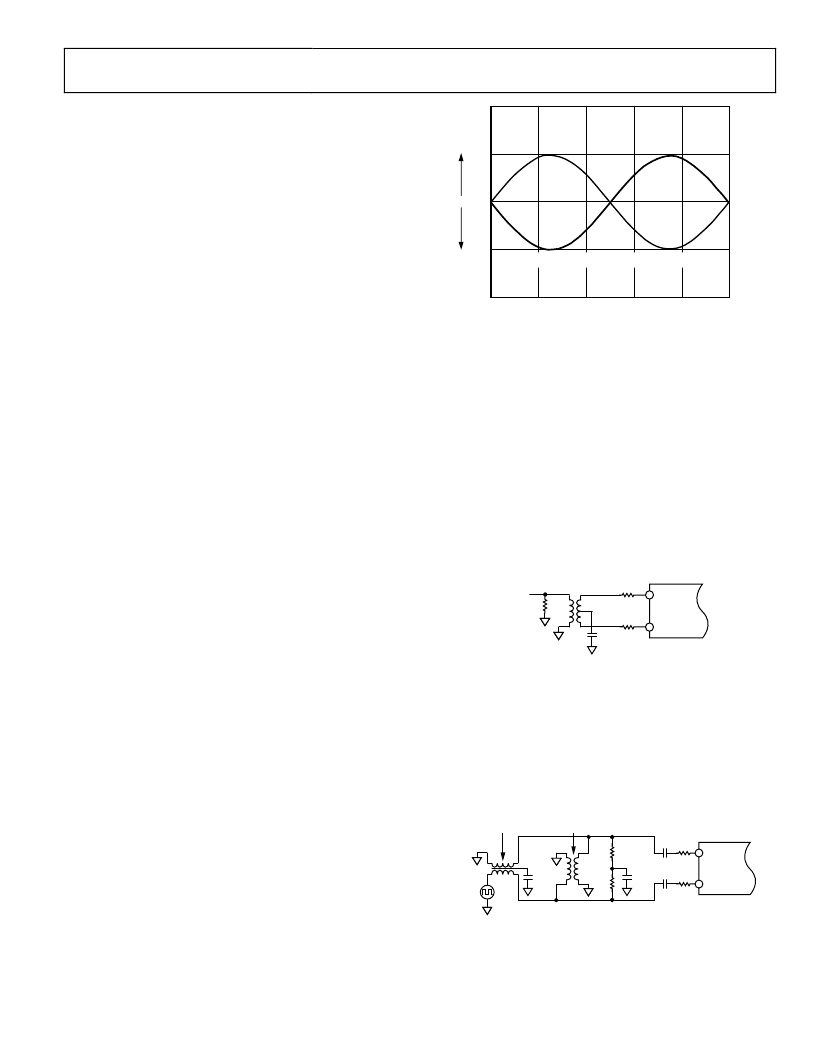
Figure 61. Differential Analog Input Range for VREF = 1.0 V
Therefore, the analog source driving the AD9445 should be ac-
coupled to the input pins. The recommended method for driving
the analog input of the AD9445 is to use an RF transformer to
convert single-ended signals to differential (see
Series resistors between the output of the transformer and the
AD9445 analog inputs help isolate the analog input source from
switching transients caused by the internal sample-and-hold
circuit. The series resistors, along with the 1 kΩ resisters connected
to the internal 3.5 V bias, must be considered in impedance
matching the transformer input. For example, if R
T
is set to
51 Ω, R
S
is set to 33 Ω, and there is a 1:1 impedance ratio trans-
former, the input will match a 50 Ω source with a full-scale drive
of 10.0 dBm. The 50 Ω impedance matching can also be incor-
porated on the secondary side of the transformer, as shown in
the evaluation board schematic (see Figure 67).
Analog Inputs
As with most new high speed, high dynamic range ADCs, the
analog input to the AD9445 is differential. Differential inputs
improve on-chip performance because signals are processed
through attenuation and gain stages. Most of the improvement
is a result of differential analog stages having high rejection of
even-order harmonics. There are also benefits at the PCB level.
First, differential inputs have high common-mode rejection of
stray signals, such as ground and power noise. Second, they
provide good rejection of common-mode signals, such as local
oscillator feedthrough. The specified noise and distortion of the
AD9445 cannot be realized with a single-ended analog input, so
such configurations are discouraged. Contact sales for
recommendations of other 14-bit ADCs that support single-
ended analog input configurations.
Figure 62).
0
0.1
μ
F
R
T
AD9445
VIN+
VIN–
R
S
R
S
ADT1–1WT
ANALOG
INPUT
SIGNAL
With the 1 V reference, which is the nominal value (see the
Internal Reference Trim section), the differential input range of
the AD9445 analog input is nominally 2.0 V p-p or 1.0 V p-p on
each input (VIN+ or VIN).
Figure 62. Transformer-Coupled Analog Input Circuit
High IF Applications
In applications where the analog input frequency range is
>100 MHz, the phase and amplitude matching at the analog
inputs becomes critical to optimize performance of the ADC.
The circuit in Figure 63 can be used to optimize the matching of
these parameters. This configuration uses a double balun config-
uration that has low parasitics, high bandwidth, and parasitic
cancellation.
The AD9445 analog input voltage range is offset from ground
by 3.5 V. Each analog input connects through a 1 kΩ resistor to
the 3.5 V bias voltage and to the input of a differential buffer.
The internal bias network on the input properly biases the
buffer for maximum linearity and range (see the
Circuits section).
Equivalent
0
0.1
μ
F
CT
AD9445
VIN+
VIN–
33
Ω
25
Ω
50
Ω
SOURCE
25
Ω
33
Ω
ETC1–1–13
ETC1–1–13
0.1
μ
F
Figure 63. Double Balun-Coupled Analog Input Circuit
相關PDF資料 |
PDF描述 |
|---|---|
| AD9446BSVZ-100 | 16-Bit, 80/100 MSPS ADC |
| AD9446BSVZ-80 | 16-Bit, 80/100 MSPS ADC |
| AD9446 | 16-Bit, 80/100 MSPS ADC |
| AD9446-100LVDS | 16-Bit, 80/100 MSPS ADC |
| AD9446-100PCB | 16-Bit, 80/100 MSPS ADC |
相關代理商/技術參數 |
參數描述 |
|---|---|
| AD9445-IF-LVDS/PCB | 制造商:Analog Devices 功能描述:Evaluation Kit For 14-Bit, 105/125 MAPA, IF Sampling ADC 制造商:Analog Devices 功能描述:EVAL KIT FOR 14BIT, 105/125 MSPS, IF SAMPLING ADC - Bulk |
| AD9445IF-LVDS/PCBZ | 制造商:Analog Devices 功能描述:Evaluation Board For AD9445IF 制造商:Analog Devices 功能描述:14-BIT 125 MSPS ADC IF EVAL BD - Bulk |
| AD9445-IF-LVDSPCB | 制造商:AD 制造商全稱:Analog Devices 功能描述:High Speed ADC USB FIFO Evaluation Kit |
| AD9445-IF-PCB | 制造商:AD 制造商全稱:Analog Devices 功能描述:14-Bit, 105/125 MSPS, IF Sampling ADC |
| AD9445XSVZ-105 | 制造商:Analog Devices 功能描述:14-BIT ADC - Trays |
發布緊急采購,3分鐘左右您將得到回復。