- 您現在的位置:買賣IC網 > PDF目錄373963 > AD9501JP (ANALOG DEVICES INC) Digitally Programmable Delay Generator PDF資料下載
參數資料
| 型號: | AD9501JP |
| 廠商: | ANALOG DEVICES INC |
| 元件分類: | 模擬信號調理 |
| 英文描述: | Digitally Programmable Delay Generator |
| 中文描述: | SPECIALTY ANALOG CIRCUIT, PQCC20 |
| 封裝: | PLASTIC, LCC-20 |
| 文件頁數: | 6/12頁 |
| 文件大小: | 180K |
| 代理商: | AD9501JP |
AD9501
REV. A
–6–
Offset between the two levels is necessary for three reasons.
First, offset allows the ramp to reset and settle without re-
entering the voltage range of the DAC. Second, the DAC may
overshoot as it switches to its most positive value (00
H
); this
could lead to false output pulses if there were no offset between
the ramp reset voltage and the upper reference. Overshoot on
the ramp could also lead to false outputs without the offset.
Finally, the ramp is slightly nonlinear for a short interval when it
is first started; the offset shifts the most positive DAC level
below this nonlinear region and maintains ramp linearity for
short programmed delay settings.
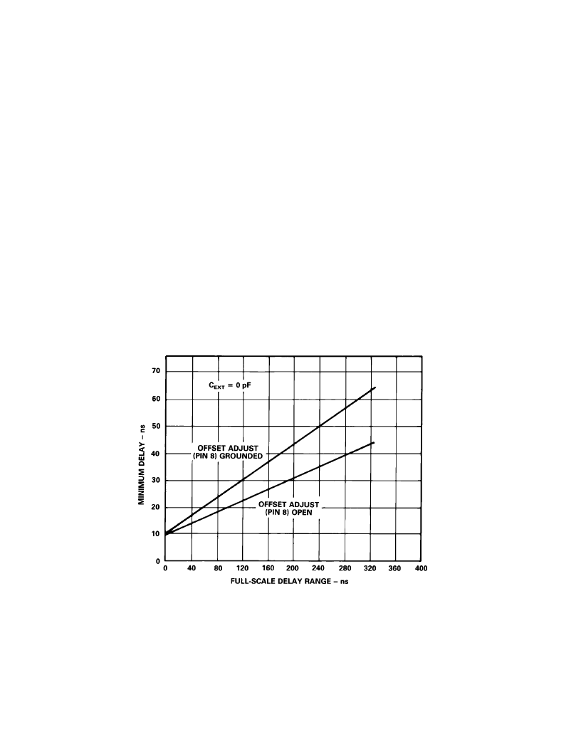
Pin 8 of the AD9501 is called OFFSET ADJUST (see block
diagram) and allows the user to control the amount of offset
separating the initial ramp voltage and the most positive DAC
reference. T his, in turn, causes the Ramp Generator delay to
vary.
Figure 2 shows differences in timing which occur if OFFSET
ADJUST Pin 8 is grounded or open. T he variable Ramp
Generator delay is the major component of the three
components which comprise Minimum Delay (t
PD
) and,
therefore, is affected by the connection to Pin 8.
It is preferable to ground Pin 8 because the smaller offset that
results from leaving it open increases the possibility of false out-
put pulses. When grounding the pin, it should be grounded
directly or connected to ground through a resistor or potentiom-
eter with a value of 10 k
or less.
Caution is urged when using resistance in series with Pin 8. T he
possibility of false output pulses, as discussed above, is in-
creased under these circumstances. Using resistance in series
with Pin 8 is recommended only when matching minimum de-
lays between two or more AD9501 devices; it is not recom-
mended if using a single AD9501. Changing the resistance
between Pin 8 and ground from zero to 10 k
varies the Ramp
Generator Delay by approximately 35%.
T he Full-Scale Delay Range (t
DFS
) can be calculated from the
equation:
(
t
DFS
)
=
R
SET
×
(
C
EX T
+
8.5
pF
)
×
3.84
Whenever Full-Scale Delay Range is 326 ns or less, C
EX T
should
be left open. Additional capacitance and/or larger values of R
SET
increase the Linear Ramp Settling T ime, which reduces the
maximum trigger rate. When delays longer than 326 ns are
required, up to 500 pF can be connected from C
EX T
to +V
S
.
R
SET
should be selected in the range from 50
to 10 k
. Graph
1 shows typical Full-Scale Delay Ranges for various values of
R
SET
and C
EX T
.
Figure 2. AD9501 Minimum Delay (t
PD
) vs. Full-Scale Delay Range (t
DFS
)
相關PDF資料 |
PDF描述 |
|---|---|
| AD9501SQ | Digitally Programmable Delay Generator |
| AD9501JQ | Digitally Programmable Delay Generator |
| AD9502 | Hybrid RS-170 Video Digitizer |
| AD9502AM | Hybrid RS-170 Video Digitizer |
| AD9502BM | Hybrid RS-170 Video Digitizer |
相關代理商/技術參數 |
參數描述 |
|---|---|
| AD9501JP-REEL | 制造商:Analog Devices 功能描述:Digitally Programmable Delay Generator 20-Pin PLCC T/R |
| AD9501JQ | 制造商:AD 制造商全稱:Analog Devices 功能描述:Digitally Programmable Delay Generator |
| AD9501SE | 制造商:Analog Devices 功能描述: |
| AD9501SE/883B | 制造商:Rochester Electronics LLC 功能描述:- Bulk |
| AD9501SQ | 制造商:AD 制造商全稱:Analog Devices 功能描述:Digitally Programmable Delay Generator |
發布緊急采購,3分鐘左右您將得到回復。