- 您現(xiàn)在的位置:買賣IC網(wǎng) > PDF目錄16533 > AD9517-0A/PCBZ (Analog Devices Inc)BOARD EVALUATION FOR AD9517-0A PDF資料下載
參數(shù)資料
| 型號: | AD9517-0A/PCBZ |
| 廠商: | Analog Devices Inc |
| 文件頁數(shù): | 1/80頁 |
| 文件大小: | 0K |
| 描述: | BOARD EVALUATION FOR AD9517-0A |
| 設計資源: | AD9517 Eval Brd Schematics AD9517 Gerber Files AD9517-0 BOM |
| 標準包裝: | 1 |
| 主要目的: | 計時,時鐘發(fā)生器 |
| 嵌入式: | 否 |
| 已用 IC / 零件: | AD9517-0A |
| 主要屬性: | 2 輸入,12 輸出,2.8GHz VCO |
| 次要屬性: | CMOS,LVPECL 和 LVDS 兼容 |
| 已供物品: | 板 |
當前第1頁第2頁第3頁第4頁第5頁第6頁第7頁第8頁第9頁第10頁第11頁第12頁第13頁第14頁第15頁第16頁第17頁第18頁第19頁第20頁第21頁第22頁第23頁第24頁第25頁第26頁第27頁第28頁第29頁第30頁第31頁第32頁第33頁第34頁第35頁第36頁第37頁第38頁第39頁第40頁第41頁第42頁第43頁第44頁第45頁第46頁第47頁第48頁第49頁第50頁第51頁第52頁第53頁第54頁第55頁第56頁第57頁第58頁第59頁第60頁第61頁第62頁第63頁第64頁第65頁第66頁第67頁第68頁第69頁第70頁第71頁第72頁第73頁第74頁第75頁第76頁第77頁第78頁第79頁第80頁
12-Output Clock Generator with
Integrated 2.8 GHz VCO
Data Sheet
Rev. E
Information furnished by Analog Devices is believed to be accurate and reliable. However, no
responsibilityisassumedbyAnalogDevicesforitsuse,norforanyinfringementsofpatentsorother
rightsofthirdpartiesthatmayresultfromitsuse.Specificationssubjecttochangewithoutnotice.No
license is granted by implication or otherwise under any patent or patent rights of Analog Devices.
Trademarksandregisteredtrademarksarethepropertyoftheirrespectiveowners.
One Technology Way, P.O. Box 9106, Norwood, MA 02062-9106, U.S.A.
Tel: 781.329.4700
2007–2013 Analog Devices, Inc. All rights reserved.
FEATURES
Low phase noise, phase-locked loop (PLL)
On-chip VCO tunes from 2.55 GHz to 2.95 GHz
External VCO/VCXO to 2.4 GHz optional
1 differential or 2 single-ended reference inputs
Reference monitoring capability
Automatic revertive and manual reference
switchover/holdover modes
Accepts LVPECL, LVDS, or CMOS references to 250 MHz
Programmable delays in path to PFD
Digital or analog lock detect, selectable
2 pairs of 1.6 GHz LVPECL outputs
Each output pair shares a 1-to-32 divider with coarse
phase delay
Additive output jitter: 225 fs rms
Channel-to-channel skew paired outputs of <10 ps
2 pairs of 800 MHz LVDS clock outputs
Each output pair shares two cascaded 1-to-32 dividers
with coarse phase delay
Additive output jitter: 275 fs rms
Fine delay adjust (Δt) on each LVDS output
Each LVDS output can be reconfigured as two 250 MHz
CMOS outputs
Automatic synchronization of all outputs on power-up
Manual output synchronization available
Available in a 48-lead LFCSP
APPLICATIONS
Low jitter, low phase noise clock distribution
10/40/100 Gb/sec networking line cards, including SONET,
Synchronous Ethernet, OTU2/3/4
Forward error correction (G.710)
Clocking high speed ADCs, DACs, DDSs, DDCs, DUCs, MxFEs
High performance wireless transceivers
ATE and high performance instrumentation
GENERAL DESCRIPTION
The AD9517-01 provides a multi-output clock distribution
function with subpicosecond jitter performance, along with an
on-chip PLL and VCO. The on-chip VCO tunes from 2.55 GHz
to 2.95 GHz. Optionally, an external VCO/VCXO of up to
2.4 GHz can be used.
The AD9517-0 emphasizes low jitter and phase noise to
maximize data converter performance, and it can benefit other
applications with demanding phase noise and jitter requirements.
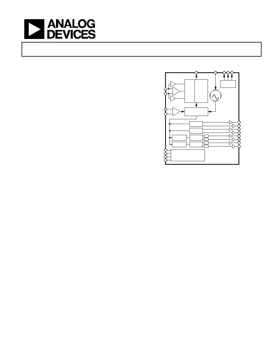
FUNCTIONAL BLOCK DIAGRAM
REFIN
REF1
REF2
CLK
LF
SW
IT
C
H
O
VER
AND
M
O
NI
T
O
R
PL
L
DIVIDER
AND MUXs
CP
VCO
STATUS
MONITOR
LVPECL
LVDS/CMOS
SERIAL CONTROL PORT
AND
DIGITAL LOGIC
AD9517-0
OUT0
OUT1
OUT2
OUT3
OUT4
OUT5
OUT6
OUT7
DIV/Φ
Δt
06424-
001
Figure 1.
The AD9517-0 features four LVPECL outputs (in two pairs)
and four LVDS outputs (in two pairs). Each LVDS output can
be reconfigured as two CMOS outputs. The LVPECL outputs
operate to 1.6 GHz, the LVDS outputs operate to 800 MHz, and
the CMOS outputs operate to 250 MHz.
For applications that require additional outputs, a crystal reference
input, zero-delay, or EEPROM for automatic configuration at
startup, the AD9520 and AD9522 are available. In addition,
a different combination of outputs.
Each pair of outputs has dividers that allow both the divide ratio
and coarse delay (or phase) to be set. The range of division for
the LVPECL outputs is 1 to 32. The LVDS/CMOS outputs allow
a range of divisions up to a maximum of 1024.
The AD9517-0 is available in a 48-lead LFCSP and can be
operated from a single 3.3 V supply. An external VCO, which
requires an extended voltage range, can be accommodated by
connecting the charge pump supply (VCP) to 5 V. A separate
LVPECL power supply can be from 2.5 V to 3.3 V (nominal).
The AD9517-0 is specified for operation over the industrial
range of 40°C to +85°C.
1
AD9517 is used throughout the data sheet to refer to all the members of the
AD9517 family. However, when AD9517-0 is used, it refers to that specific
member of the AD9517 family.
相關PDF資料 |
PDF描述 |
|---|---|
| AD9517-1A/PCBZ | BOARD EVALUATION FOR AD9517-1A |
| VI-J02-EZ-S | CONVERTER MOD DC/DC 15V 25W |
| 1062672021 | F/O CABLE MTP/JMPR (2) 500MM |
| AD9517-2A/PCBZ | BOARD EVALUATION FOR AD9517-2A |
| VI-J00-EZ-S | CONVERTER MOD DC/DC 5V 25W |
相關代理商/技術參數(shù) |
參數(shù)描述 |
|---|---|
| AD9517-0BCPZ | 制造商:Analog Devices 功能描述: |
| AD9517-1 | 制造商:AD 制造商全稱:Analog Devices 功能描述:12-Output Clock Generator with Integrated 2.5 GHz VCO |
| AD9517-1A/PCBZ | 功能描述:BOARD EVALUATION FOR AD9517-1A RoHS:是 類別:編程器,開發(fā)系統(tǒng) >> 評估演示板和套件 系列:- 標準包裝:1 系列:- 主要目的:電信,線路接口單元(LIU) 嵌入式:- 已用 IC / 零件:IDT82V2081 主要屬性:T1/J1/E1 LIU 次要屬性:- 已供物品:板,電源,線纜,CD 其它名稱:82EBV2081 |
| AD9517-1ABCPZ | 功能描述:IC CLOCK GEN 2.5GHZ VCO 48LFCSP RoHS:是 類別:集成電路 (IC) >> 時鐘/計時 - 時鐘發(fā)生器,PLL,頻率合成器 系列:- 標準包裝:1,000 系列:Precision Edge® 類型:時鐘/頻率合成器 PLL:無 輸入:CML,PECL 輸出:CML 電路數(shù):1 比率 - 輸入:輸出:2:1 差分 - 輸入:輸出:是/是 頻率 - 最大:10.7GHz 除法器/乘法器:無/無 電源電壓:2.375 V ~ 3.6 V 工作溫度:-40°C ~ 85°C 安裝類型:表面貼裝 封裝/外殼:16-VFQFN 裸露焊盤,16-MLF? 供應商設備封裝:16-MLF?(3x3) 包裝:帶卷 (TR) 其它名稱:SY58052UMGTRSY58052UMGTR-ND |
| AD9517-1ABCPZ-RL7 | 功能描述:IC CLOCK GEN 2.5GHZ VCO 48LFCSP RoHS:是 類別:集成電路 (IC) >> 時鐘/計時 - 時鐘發(fā)生器,PLL,頻率合成器 系列:- 標準包裝:2,000 系列:- 類型:PLL 時鐘發(fā)生器 PLL:帶旁路 輸入:LVCMOS,LVPECL 輸出:LVCMOS 電路數(shù):1 比率 - 輸入:輸出:2:11 差分 - 輸入:輸出:是/無 頻率 - 最大:240MHz 除法器/乘法器:是/無 電源電壓:3.135 V ~ 3.465 V 工作溫度:0°C ~ 70°C 安裝類型:表面貼裝 封裝/外殼:32-LQFP 供應商設備封裝:32-TQFP(7x7) 包裝:帶卷 (TR) |
發(fā)布緊急采購,3分鐘左右您將得到回復。