- 您現在的位置:買賣IC網 > PDF目錄373964 > AD9621AN (ANALOG DEVICES INC) Wideband Voltage Feedback Amplifier PDF資料下載
參數資料
| 型號: | AD9621AN |
| 廠商: | ANALOG DEVICES INC |
| 元件分類: | 運動控制電子 |
| 英文描述: | Wideband Voltage Feedback Amplifier |
| 中文描述: | OP-AMP, 15000 uV OFFSET-MAX, 350 MHz BAND WIDTH, PDIP8 |
| 封裝: | PLASTIC, DIP-8 |
| 文件頁數: | 4/6頁 |
| 文件大小: | 305K |
| 代理商: | AD9621AN |
AD9621
REV. 0
–4–
phase margin (55
°
), low noise current (3.6 pA/
√
Hz
), and slew
rate (1200 V/
μ
s) give higher performance capabilities to these
applications over previous voltage feedback designs.
With a settling time of 11 ns to 0.01% and 7 ns to 0.1%, the de-
vice is an excellent choice for DAC I/V conversion. The same
characteristics, along with low harmonic distortion, make it a
good choice for ADC buffering/amplification. With its superb
linearity at relatively high signal frequencies, it is an ideal driver
for ADCs up to 14 bits.
Layout Considerations
As with all wide bandwidth components, printed circuit layout
is critical to obtain best dynamic performance with the AD9621.
The ground plane in the area of the amplifier and its associated
components should cover as much of the component side of the
board as possible (or first interior layer of a multi layer surface
mount board).
The ground plane should be removed in the area of the inputs
and R
F
and R
G
to minimize stray capacitance at the input. The
same precaution should be used for C
B
, if used. Each power
supply trace should be decoupled close to the package with a
0.1
μ
F ceramic capacitor, plus a 6.8
μ
F tantalum nearby.
All lead lengths for input, output, and feedback resistor should
be kept as short as possible. All gain setting resistors should be
chosen for low values of parasitic capacitance and inductance,
i.e., microwave resistors and/or carbon resistors.
Microstrip techniques should be used for lead lengths in excess
of one inch. Sockets should be avoided if at all possible because
of their high series inductance. If sockets are necessary, indi-
vidual pin sockets such as AMP p/n 6-330808-3 should be used.
These contribute far less stray reactance than molded socket
assemblies.
An evaluation board is available from Analog Devices for a
nominal charge.
Pulse Response
Unlike a traditional voltage feedback amplifier in which slew
speed is dictated by its front end dc quiescent current and gain
bandwidth product, the AD9621 provides “on demand” trans-
conductance current that increases proportionally to the input
“step” signal amplitude. This results in slew speeds (1200 V/
μ
s)
comparable to wideband current feedback designs. This, com-
bined with relatively low input noise current (3.6 pA/
√
Hz
), gives
the AD9621 the best attributes of both voltage and current feed-
back amplifiers.
Bootstrap Capacitor (C
B
)
In most applications, the C
B
capacitor will not be required.
Under certain conditions, it can be used to further enhance set-
tling time performance.
The C
B
capacitor (0.001
μ
F) connects to the internal high im-
pedance nodes of the amplifier. Using this capacitor will reduce
the large signal (4 V) step output settling time by 3 to 5 ns for
0.05% or greater accuracy. For settling accuracy less than
0.05% or for smaller step sizes, its effect will be less apparent.
Under heavy slew conditions, this capacitor forces the internal
signal (initial step) amplitude to be controlled by the “on”
(slewed) transistor, preventing its complement from completely
turning off. This allows for faster settling time of these internal
nodes and also the output.
In the frequency domain, total (high frequency) distortion will
be approximately the same with or without C
B
. Typically, the
3rd harmonic will be greater than the 2nd without C
B
. This will
be reversed with C
B
in place.
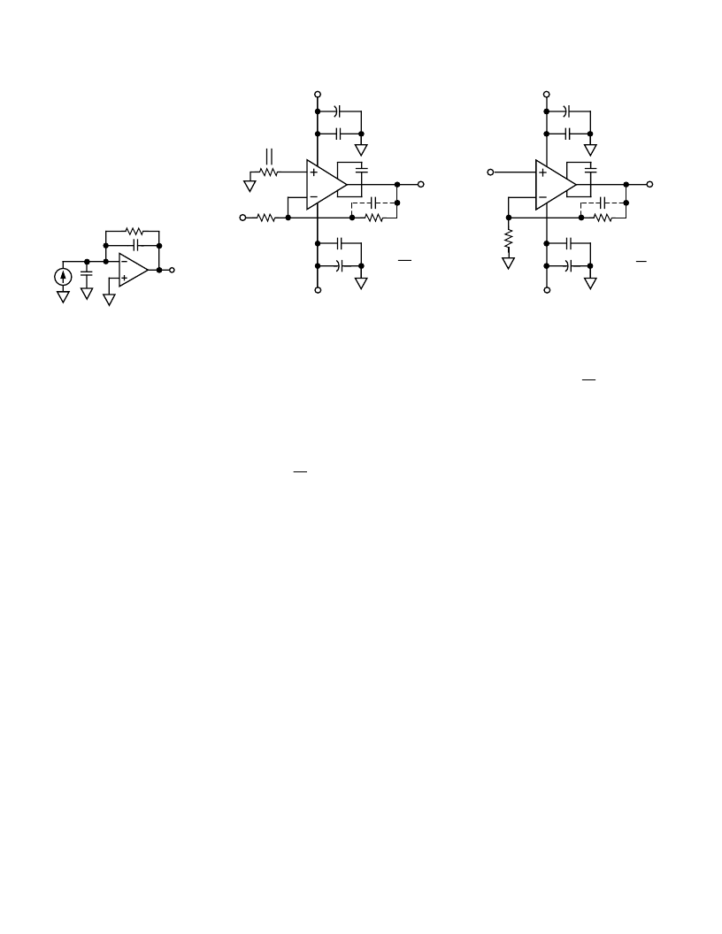
APPLICATIONS
The AD9621 is a voltage feedback amplifier and is well suited
for such applications as photo-detector preamp, active filters,
and log amplifiers. The device’s wide bandwidth (350 MHz),
R
F
C
F
C
I
V
OUT
Figure 1. Transimpedance
Configuration
2
3
4
7
6
0.1
μ
F
0.1
μ
F
1
8
6.8
μ
F
R
G
V
IN
6.8
μ
F
+V
S
–V
S
C
B (OPTIONAL)
C
F
V
OUT
R
F
500
A
V
= 1+ R
F
R
G
Figure 3. Noninverting Gain Connection
Diagram
2
3
4
7
6
0.1
μ
F
0.1
μ
F
1
8
6.8
μ
F
R
F
R
G
R
G
V
IN
6.8
μ
F
+V
S
–V
S
C
B (OPTIONAL)
C
F
V
OUT
R
F
500
A
V
= –R
F
R
G
Figure 2. Inverting Gain Connection
Diagram
相關PDF資料 |
PDF描述 |
|---|---|
| AD9621AQ | Wideband Voltage Feedback Amplifier |
| AD9621AR | Wideband Voltage Feedback Amplifier |
| AD9621SQ | Wideband Voltage Feedback Amplifier |
| AD9630 | Low Distortion 750 MHz Closed-Loop Buffer Amp |
| AD9630AN | Low Distortion 750 MHz Closed-Loop Buffer Amp |
相關代理商/技術參數 |
參數描述 |
|---|---|
| AD9621AQ | 制造商:AD 制造商全稱:Analog Devices 功能描述:Wideband Voltage Feedback Amplifier |
| AD9621AR | 制造商:AD 制造商全稱:Analog Devices 功能描述:Wideband Voltage Feedback Amplifier |
| AD9621SQ | 制造商:AD 制造商全稱:Analog Devices 功能描述:Wideband Voltage Feedback Amplifier |
| AD9622 | 制造商:AD 制造商全稱:Analog Devices 功能描述:Wideband Voltage Feedback Amplifier |
| AD9622AN | 制造商:Rochester Electronics LLC 功能描述:- Bulk |
發布緊急采購,3分鐘左右您將得到回復。