- 您現在的位置:買賣IC網 > PDF目錄1988 > AD9633BCPZRL7-105 (Analog Devices Inc)IC ADC 12BIT SRL 105MSPS 48LFCSP PDF資料下載
參數資料
| 型號: | AD9633BCPZRL7-105 |
| 廠商: | Analog Devices Inc |
| 文件頁數: | 1/40頁 |
| 文件大小: | 0K |
| 描述: | IC ADC 12BIT SRL 105MSPS 48LFCSP |
| 標準包裝: | 750 |
| 位數: | 12 |
| 采樣率(每秒): | 105M |
| 數據接口: | LVDS,串行,SPI? |
| 轉換器數目: | 4 |
| 功率耗散(最大): | 473mW |
| 電壓電源: | 模擬和數字 |
| 工作溫度: | -40°C ~ 85°C |
| 安裝類型: | 表面貼裝 |
| 封裝/外殼: | 48-WFQFN 裸露焊盤,CSP |
| 供應商設備封裝: | 48-LFCSP-WQ(7x7) |
| 包裝: | 帶卷 (TR) |
| 輸入數目和類型: | 4 個差分,雙極 |
當前第1頁第2頁第3頁第4頁第5頁第6頁第7頁第8頁第9頁第10頁第11頁第12頁第13頁第14頁第15頁第16頁第17頁第18頁第19頁第20頁第21頁第22頁第23頁第24頁第25頁第26頁第27頁第28頁第29頁第30頁第31頁第32頁第33頁第34頁第35頁第36頁第37頁第38頁第39頁第40頁
Quad, 12-Bit, 80 MSPS/105 MSPS/
125 MSPS, Serial LVDS 1.8 V ADC
Data Sheet
Rev. 0
Information furnished by Analog Devices is believed to be accurate and reliable. However, no
responsibilityis assumedbyAnalogDevicesforitsuse,norforanyinfringementsof patentsorother
rightsofthirdpartiesthatmayresultfromitsuse.Specificationssubjecttochangewithoutnotice.No
license is granted by implication or otherwise under any patent or patent rights of Analog Devices.
Trademarksandregisteredtrademarksarethepropertyoftheirrespectiveowners.
One Technology Way, P.O. Box 9106, Norwood, MA 02062-9106, U.S.A.
Tel: 781.329.4700
www.analog.com
Fax: 781.461.3113
2011 Analog Devices, Inc. All rights reserved.
FEATURES
1.8 V supply operation
Low power: 100 mW per channel at 125 MSPS with scalable
power options
SNR = 71 dB (to Nyquist)
SFDR = 91 dBc (to Nyquist)
DNL = ±0.3 LSB (typical); INL = ±0.5 LSB (typical)
Serial LVDS (ANSI-644, default) and low power, reduced
signal option (similar to IEEE 1596.3)
650 MHz full power analog bandwidth
2 V p-p input voltage range
Serial port control
Full chip and individual channel power-down modes
Flexible bit orientation
Built-in and custom digital test pattern generation
Multichip sync and clock divider
Programmable output clock and data alignment
Programmable output resolution
Standby mode
APPLICATIONS
Medical ultrasound
High speed imaging
Quadrature radio receivers
Diversity radio receivers
Test equipment
GENERAL DESCRIPTION
The AD9633 is a quad, 12-bit, 80 MSPS/105 MSPS/125 MSPS
analog-to-digital converter (ADC) with an on-chip sample-and-
hold circuit designed for low cost, low power, small size, and
ease of use. The product operates at a conversion rate of up to
125 MSPS and is optimized for outstanding dynamic performance
and low power in applications where a small package size is
critical.
The ADC requires a single 1.8 V power supply and LVPECL-/
CMOS-/LVDS-compatible sample rate clock for full performance
operation. No external reference or driver components are
required for many applications.
The ADC automatically multiplies the sample rate clock for the
appropriate LVDS serial data rate. A data clock output (DCO) for
capturing data on the output and a frame clock output (FCO)
for signaling a new output byte are provided. Individual-channel
power-down is supported and typically consumes less than 2 mW
when all channels are disabled.
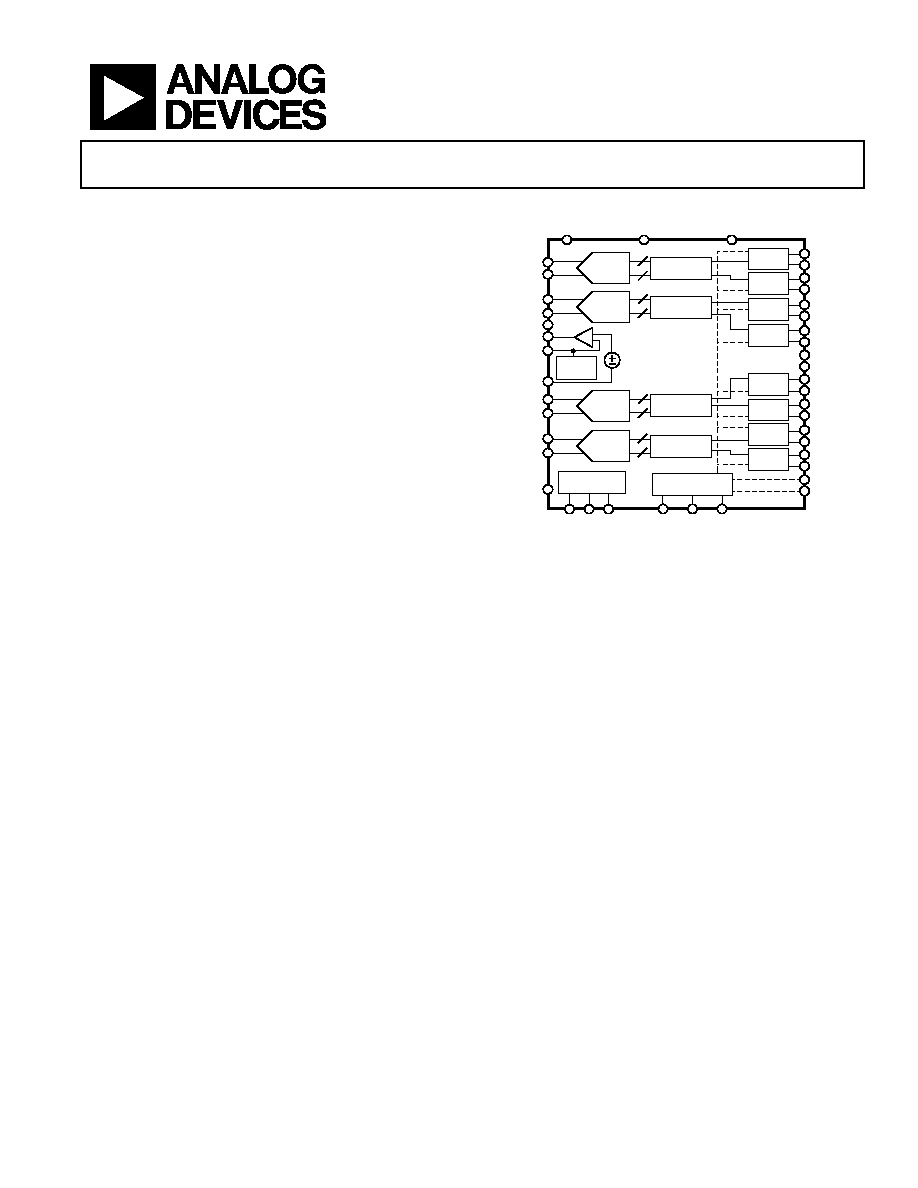
FUNCTIONAL BLOCK DIAGRAM
AD9633
AVDD
PDWN
DRVDD
REF
SELECT
VIN–A
VIN+A
VIN–B
RBIAS
VIN+B
VIN–D
VIN+D
VIN–C
VIN+C
SENSE
AGND
VCM
VREF
D0–A
D0+A
D0–B
D0+B
D1–B
D1+B
D1–C
D1+C
D0–C
D0+C
D1–D
D1+D
DCO–
DCO+
D0–D
D0+D
FCO–
FCO+
D1–A
D1+A
CS
B
S
D
IO/OLM
SC
L
K
/D
T
P
PIPELINE
ADC
PIPELINE
ADC
PIPELINE
ADC
SERIAL
LVDS
DIGITAL
SERIALIZER
DIGITAL
SERIALIZER
DIGITAL
SERIALIZER
DIGITAL
SERIALIZER
SERIAL PORT
INTERFACE
SERIAL
LVDS
SERIAL
LVDS
SERIAL
LVDS
SERIAL
LVDS
SERIAL
LVDS
SERIAL
LVDS
SERIAL
LVDS
PIPELINE
ADC
12
1V
10
073
-00
1
SY
N
C
CL
K
+
CL
K
–
CLOCK
MANAGEMENT
Figure 1.
The ADC contains several features designed to maximize
flexibility and minimize system cost, such as programmable
output clock and data alignment and digital test pattern
generation. The available digital test patterns include built-in
deterministic and pseudorandom patterns, along with custom user-
defined test patterns entered via the serial port interface (SPI).
The AD9633 is available in a RoHS-compliant, 48-lead LFCSP.
It is specified over the industrial temperature range of 40°C to
+85°C. This product is protected by a U.S. patent.
PRODUCT HIGHLIGHTS
1.
Small Footprint. Four ADCs are contained in a small, space-
saving package.
2.
Low power of 100 mW/channel at 125 MSPS with scalable
power options.
3.
Pin compatible to the AD9253 14-bit quad ADC.
4.
Ease of Use. A data clock output (DCO) operates at
frequencies of up to 375 MHz and supports double data
rate (DDR) operation.
5.
User Flexibility. The SPI control offers a wide range of flexible
features to meet specific system requirements.
相關PDF資料 |
PDF描述 |
|---|---|
| AD9634BCPZRL7-170 | IC ADC 12BIT SRL 170MSPS 32LFCSP |
| AD9637BCPZRL7-80 | IC ADC 12BIT SRL 80MSPS 64LFCSP |
| AD9639BCPZ-170 | IC ADC 12B 170MSPS QUAD 72LFCSP |
| AD9640ABCPZ-125 | IC ADC 14BIT 125MSPS 64LFCSP |
| AD9641BCPZ-80 | IC ADC 14BIT SRL 80MSPS 32LFCSP |
相關代理商/技術參數 |
參數描述 |
|---|---|
| AD9633BCPZRL7-125 | 功能描述:模數轉換器 - ADC 12 bit 125msps low pwr quad ADC RoHS:否 制造商:Analog Devices 通道數量: 結構: 轉換速率: 分辨率: 輸入類型: 信噪比: 接口類型: 工作電源電壓: 最大工作溫度: 安裝風格: 封裝 / 箱體: |
| AD9633BCPZRL7-80 | 功能描述:IC ADC 12BIT SRL 80MSPS 48LFCSP RoHS:是 類別:集成電路 (IC) >> 數據采集 - 模數轉換器 系列:- 標準包裝:1 系列:- 位數:14 采樣率(每秒):83k 數據接口:串行,并聯 轉換器數目:1 功率耗散(最大):95mW 電壓電源:雙 ± 工作溫度:0°C ~ 70°C 安裝類型:通孔 封裝/外殼:28-DIP(0.600",15.24mm) 供應商設備封裝:28-PDIP 包裝:管件 輸入數目和類型:1 個單端,雙極 |
| AD9634 | 制造商:AD 制造商全稱:Analog Devices 功能描述:12-Bit, 170 MSPS/210 MSPS/250 MSPS |
| AD9634-170EBZ | 功能描述:數據轉換 IC 開發工具 12 Bit 170 Msps ADC RoHS:否 制造商:Texas Instruments 產品:Demonstration Kits 類型:ADC 工具用于評估:ADS130E08 接口類型:SPI 工作電源電壓:- 6 V to + 6 V |
| AD9634-210EBZ | 功能描述:數據轉換 IC 開發工具 12 Bit 210 Msps ADC RoHS:否 制造商:Texas Instruments 產品:Demonstration Kits 類型:ADC 工具用于評估:ADS130E08 接口類型:SPI 工作電源電壓:- 6 V to + 6 V |
發布緊急采購,3分鐘左右您將得到回復。