- 您現在的位置:買賣IC網 > PDF目錄373965 > AD9698KN (ANALOG DEVICES INC) Ultrafast TTL Comparators PDF資料下載
參數資料
| 型號: | AD9698KN |
| 廠商: | ANALOG DEVICES INC |
| 元件分類: | 運動控制電子 |
| 英文描述: | Ultrafast TTL Comparators |
| 中文描述: | DUAL COMPARATOR, 3000 uV OFFSET-MAX, PDIP16 |
| 封裝: | PLASTIC, DIP-16 |
| 文件頁數: | 5/8頁 |
| 文件大小: | 135K |
| 代理商: | AD9698KN |
AD9696/AD9698
–5–
REV. B
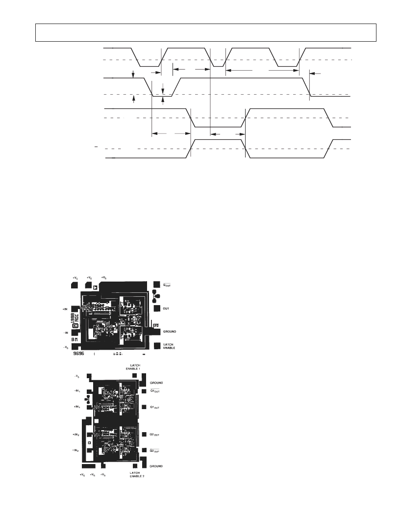
t
H
50%
50%
LATCH
ENABLE
DIFFERENTIAL
INPUT VOLTAGE
Q
TWO DIODES
ABOVE GROUND
LATCH
COMPARE
Q
t
PD
t
PD (E)
V
OS
– MINIMUM SETUP TIME (Typically 1.7ns)
– MINIMUM HOLD TIME (Typically 1.9ns)
– INPUT TO OUTPUT DELAY
– LATCH ENABLE TO OUTPUT DELAY
t
H
t
PD
t
S
t
PD (E)
– MINIMUM LATCH ENABLE PULSE WIDTH (Typically 2.5ns)
– INPUT OFFSET VOLTAGE
– OVERDRIVE VOLTAGE
V
OS
V
OD
t
PW (E)
V
OD
V
IN
t
PW (E)
t
S
AD9696/AD9698 Timing Diagram
DIE LAY OUT AND ME CHANICAL INFORMAT ION
Die Dimensions AD9696 . . . . . . . . . . . . . 59
×
71
×
15 (
±
2) mils
AD9698 . . . . . . . . . . . . 79
×
109
×
15 (
±
2) mils
Pad Dimensions . . . . . . . . . . . . . . . . . . . . . . . . . . . . . 4
×
4 mils
Metalization . . . . . . . . . . . . . . . . . . . . . . . . . . . . . . Aluminum
Backing . . . . . . . . . . . . . . . . . . . . . . . . . . . . . . . . . . . . . None
Substrate Potential . . . . . . . . . . . . . . . . . . . . . . . . . . . . . . . –V
S
Passivation . . . . . . . . . . . . . . . . . . . . . . . . . . . . . . . . . . Nitride
T HE ORY OF OPE RAT ION
Refer to the block diagram of the AD9696/AD9698 compara-
tors. T he AD9696 and AD9698 T T L voltage comparator archi-
tecture consists of five basic stages: input, latch, gain, level shift
and output. Each stage is designed to provide optimal perfor-
mance and make it easy to use the comparators.
T he input stage operates with either a single +5-volt supply, or
with a +5-volt supply and a –5.2-volt supply. For optimum
power efficiency, the remaining stages operate with only a single
+5-volt supply. T he input stage is an input differential pair
without the customary emitter follower buffers. T his configura-
tion increases input bias currents but maximizes the input volt-
age range.
A latch stage allows the most recent output state to be retained
as long as the latch input is held high. In this way, the input to
the comparator can be changed without any change in the out-
put state. As soon as the latch enable input is switched to LOW,
the output changes to the new value dictated by the signal ap-
plied to the input stage.
T he gain stage assures that even with small values of input volt-
age, there will be sufficient levels applied to the following stages
to cause the output to switch T T L states as required. A level
shift stage between the gain stage and the T T L output stage
guarantees that appropriate voltage levels are applied from the
gain stage to the T T L output stage.
Only the output stage uses T T L logic levels; this minimum use
of T T L circuits maximizes speed and minimizes power con-
sumption. T he outputs are clamped with Schottky diodes to as-
sure that the rising and falling edges of the output signal are
closely matched.
T he AD9696 and AD9698 represent the state of the art in high
speed T T L voltage comparators. Great care has been taken to
optimize the propagation delay dispersion performance. T his as-
sures that the output delays will remain constant despite varying
levels of input overdrive. T his characteristic, along with closely
matched rising and falling outputs, provides extremely consis-
tent results at previously unattainable speeds.
相關PDF資料 |
PDF描述 |
|---|---|
| AD9698KQ | Ultrafast TTL Comparators |
| AD9698KR | Ultrafast TTL Comparators |
| AD9698TQ | Ultrafast TTL Comparators |
| AD9696 | Ultrafast TTL Comparators |
| AD9696KN | Ultrafast TTL Comparators |
相關代理商/技術參數 |
參數描述 |
|---|---|
| AD9698KQ | 制造商:AD 制造商全稱:Analog Devices 功能描述:Ultrafast TTL Comparators |
| AD9698KR | 制造商:AD 制造商全稱:Analog Devices 功能描述:Ultrafast TTL Comparators |
| AD9698TQ | 制造商:AD 制造商全稱:Analog Devices 功能描述:Ultrafast TTL Comparators |
| AD9698TQ/883B | 制造商:未知廠家 制造商全稱:未知廠家 功能描述:Analog Comparator |
| AD9698TZ/883B | 制造商:AD 制造商全稱:Analog Devices 功能描述:Ultrafast TTL Comparators |
發布緊急采購,3分鐘左右您將得到回復。