- 您現在的位置:買賣IC網 > PDF目錄373965 > AD9708-EB (Analog Devices, Inc.) 8-Bit, 100 MSPS TxDAC D/A Converter PDF資料下載
參數資料
| 型號: | AD9708-EB |
| 廠商: | Analog Devices, Inc. |
| 英文描述: | 8-Bit, 100 MSPS TxDAC D/A Converter |
| 中文描述: | 8位,100 MSPS的TxDAC系列D / A轉換 |
| 文件頁數: | 9/16頁 |
| 文件大小: | 246K |
| 代理商: | AD9708-EB |
AD9708
–9–
REV. B
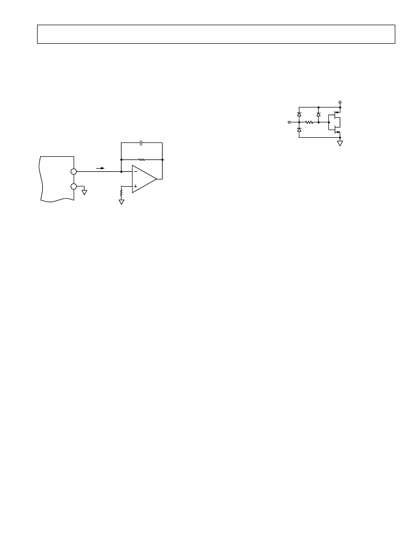
voltage. Figure 17 shows a buffered singled-ended output con-
figuration in which the op amp, U1, performs an I-V conversion
on the AD9708 output current. U1 provides a negative unipolar
output voltage and its full-scale output voltage is simply the
product of R
FB
and I
OUTFS
. The full-scale output should be set
within U1’s voltage output swing capabilities by scaling I
OUTFS
and/or R
FB
. An improvement in ac distortion performance may
result with a reduced I
OUTFS
, since the signal current U1 will be
required to sink and will be subsequently reduced. Note, the ac
distortion performance of this circuit at higher DAC update
rates may be limited by U1’s slewing capabilities.
AD9708
22
IOUTA
IOUTB
21
C
OPT
200
V
U1
V
OUT
= I
OUTFS
3
R
FB
I
OUTFS
= 10mA
R
FB
200
V
Figure 17. Unipolar Buffered Voltage Output
IOUTA and IOUTB also have a negative and positive voltage
compliance range that must be adhered to in order to achieve
optimum performance. The positive output compliance range is
slightly dependent on the full-scale output current, I
OUTFS
. It
degrades slightly from its nominal 1.25 V for an I
OUTFS
= 20 mA
to 1.00 V for an I
OUTFS
= 2 mA. Applications requiring the
AD9708’s output (i.e., V
OUTA
and/or V
OUTB
) to extend up to its
output compliance range should size R
LOAD
accordingly. Operation
beyond this compliance range will adversely affect the AD9708’s
linearity.
The differential voltage, V
DIFF
, existing between V
OUTA
and
V
OUTB
may also be converted to a single-ended voltage via a
transformer or differential amplifier configuration. Refer to the
DIFFERENTIAL OUTPUT CONFIGURATION section for
more information.
DIGITAL INPUTS
The AD9708’s digital input consists of eight data input pins and
a clock input pin. The 8-bit parallel data inputs follow standard
positive binary coding where DB7 is the most significant bit
(MSB) and DB0 is the least significant bit (LSB). The digital
interface is implemented using an edge-triggered master slave
latch. The DAC output is updated following the rising edge of
the clock as shown in Figure 1 and is designed to support a
clock rate as high as 125 MSPS. The clock can be operated at
any duty cycle that meets the specified latch pulsewidth. The
setup-and-hold times can also be varied within the clock cycle as
long as the specified minimum times are met; although the
location of these transition edges may affect digital feedthrough
and distortion performance.
The digital inputs are CMOS compatible with logic thresholds,
V
THRESHOLD
set to approximately half the digital positive supply
(DVDD) or
V
THRESHOLD
= DVDD
/2 (
±
20%)
Figure 18 shows the equivalent digital input circuit for the data
and clock inputs. The sleep mode input is similar, except that
it contains an active pull-down circuit, thus ensuring that the
AD9708 remains enabled if this input is left disconnected. The
internal digital circuitry of the AD9708 is capable of operating
over a digital supply range of 2.7 V to 5.5 V. As a result, the
digital inputs can also accommodate TTL levels when DVDD is
set to accommodate the maximum high level voltage, V
OH(MAX)
,
of the TTL drivers. A DVDD of 3 V to 3.3 V will typically
ensure upper compatibility of most TTL logic families.
DVDD
DIGITAL
INPUT
Figure 18. Equivalent Digital Input
Since the AD9708 is capable of being updated up to 125 MSPS,
the quality of the clock and data input signals are important in
achieving the optimum performance. The drivers of the digital
data interface circuitry should be specified to meet the minimum
setup-and-hold times of the AD9708 as well as its required min/
max input logic level thresholds. Typically, the selection of the
slowest logic family that satisfies the above conditions will result
in the lowest data feedthrough and noise.
Digital signal paths should be kept short and run lengths matched
to avoid propagation delay mismatch. The insertion of a low
value resistor network (i.e., 20
to 100
) between the AD9708
digital inputs and driver outputs may be helpful in reducing any
overshooting and ringing at the digital inputs that contribute to
data feedthrough. For longer run lengths and high data update
rates, strip line techniques with proper termination resistors
should be considered to maintain “clean” digital inputs. Also,
operating the AD9708 with reduced logic swings and a corre-
sponding digital supply (DVDD) will also reduce data feedthrough.
The external clock driver circuitry should provide the AD9708
with a low jitter clock input meeting the min/max logic levels
while providing fast edges. Fast clock edges will help minimize
any jitter that will manifest itself as phase noise on a recon-
structed waveform. However, the clock input could also be
driven by via a sine wave, which is centered around the digital
threshold (i.e., DVDD/2), and meets the min/max logic threshold.
This may result in a slight degradation in the phase noise, which
becomes more noticeable at higher sampling rates and output
frequencies. Note, at higher sampling rates the 20% tolerance
of the digital logic threshold should be considered since it will
affect the effective clock duty cycle and subsequently cut into
the required data setup-and-hold times.
SLEEP MODE OPERATION
The AD9708 has a power-down function that turns off the
output current and reduces the supply current to less than 8.5mA
over the specified supply range of 2.7V to 5.5 V and tempera-
ture range. This mode can be activated by applying a logic level
“1” to the SLEEP pin. This digital input also contains an active
pull-down circuit that ensures the AD9708 remains enabled if
this input is left disconnected. The SLEEP input with active
pull-down requires <40
μ
A of drive current.
The power-up and power-down characteristics of the AD9708
are dependent on the value of the compensation capacitor con-
nected to COMP2 (Pin 23). With a nominal value of 0.1
μ
F, the
AD9708 takes less than 5
μ
s to power down and approximately
3.25 ms to power back up.
相關PDF資料 |
PDF描述 |
|---|---|
| AD9708AR | 8-Bit, 100 MSPS TxDAC D/A Converter |
| AD9708ARU | 8-Bit, 100 MSPS TxDAC D/A Converter |
| AD9708* | 1A Low Noise High Current LED Charge Pump with Independent Torch/Flash Current Control; Package: DFN; No of Pins: 12; Temperature Range: -40°C to +125°C |
| AD9708 | 8-Bit, 100 MSPS TxDAC D/A Converter |
| AD9709 | 8-Bit, 125 MSPS Dual TxDAC D/A Converter |
相關代理商/技術參數 |
參數描述 |
|---|---|
| AD9708-EBZ | 功能描述:BOARD EVAL FOR AD9708 RoHS:是 類別:編程器,開發系統 >> 評估板 - 數模轉換器 (DAC) 系列:TxDAC® 產品培訓模塊:Lead (SnPb) Finish for COTS Obsolescence Mitigation Program 標準包裝:1 系列:- DAC 的數量:4 位數:12 采樣率(每秒):- 數據接口:串行,SPI? 設置時間:3µs DAC 型:電流/電壓 工作溫度:-40°C ~ 85°C 已供物品:板 已用 IC / 零件:MAX5581 |
| AD9709 | 制造商:AD 制造商全稱:Analog Devices 功能描述:Analog Devices: Data Converters: DAC 8-Bit, 10 ns to 100 ns Converters Selection Table |
| AD9709_09 | 制造商:AD 制造商全稱:Analog Devices 功能描述:8-Bit, 125 MSPS, Dual TxDAC Digital-to-Analog Converter |
| AD9709ASF | 制造商:Analog Devices 功能描述:8BIT DUAL DAC W/POLY FUSE CALIBRATION - Bulk |
| AD9709AST | 制造商:Analog Devices 功能描述:DAC 2-CH Segment 8-bit 48-Pin LQFP 制造商:Rochester Electronics LLC 功能描述:8-BIT 125 MSPS DUAL TXDAC+ D/A CONVERTER - Bulk 制造商:Analog Devices 功能描述:D/A Converter (D-A) IC |
發布緊急采購,3分鐘左右您將得到回復。