- 您現(xiàn)在的位置:買賣IC網(wǎng) > PDF目錄373968 > AD9834BRU (ANALOG DEVICES INC) Low Power, +2.3 V to +5.5 V, 50 MHz Complete DDS PDF資料下載
參數(shù)資料
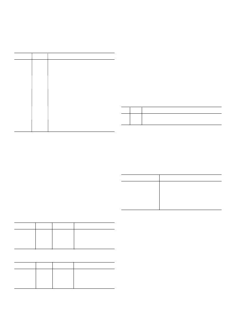
| 型號: | AD9834BRU |
| 廠商: | ANALOG DEVICES INC |
| 元件分類: | 數(shù)字信號處理外設(shè) |
| 英文描述: | Low Power, +2.3 V to +5.5 V, 50 MHz Complete DDS |
| 中文描述: | DSP-NUM CONTROLLED OSCILLATOR, PDSO20 |
| 封裝: | ROHS COMPLAINT, MO-153AC, TSSOP-20 |
| 文件頁數(shù): | 12/20頁 |
| 文件大小: | 236K |
| 代理商: | AD9834BRU |
AD9834
The Frequency and Phase Resisters
The AD9834 contains 2 frequency registers and 2 phase
registers. These are described in Table 3 below.
–
12
–
REV PrM
PRELIMINARY TECHNICAL DATA
Table 3. Frequency/Phase Registers
Register
Size
Description
FREQ0
28 Bits
Frequency Register 0. When FSEL
bit or FSELECT pin = 0, this regis-
ter defines the output frequency as a
fraction of the MCLK frequency.
Frequency Register 1. When FSEL
bit or FSELECT pin = 1, this regis-
ter defines the output frequency as a
fraction of the MCLK frequency.
Phase Offset Register 0. When PSEL
bit or PSELECT pin = 0, the con-
tents of this register are added to the
output of the phase accumulator.
Phase Offset Register 1. When PSEL
bit or PSELECT pin = 1, the con-
tents of this register are added to the
output of the phase accumulator.
FREQ1
28 Bits
PHASE0
12 Bits
PHASE1
12 Bits
The analog output from the AD9834 is
f
MCLK
/2
28
x FREQREG
where FREQREG is the value loaded into the selected
frequency register. This signal will be phase shifted by
2
π
/4096 x PHASEREG
where PHASEREG is the value contained in the selected
phase register.
Access to the frequency and phase registers is controlled
by both the FSELECT/PSELECT pins and the FSEL/
PSEL control bits. If the control bit PIN/SW = 1, the
pins controls the function, whereas if PIN/SW = 0, the
bits control the function. This is outlined in tables 4 and 5
below. If the FSEL/PSEL bits are being used, the pins
should preferably be held at CMOS logic high or low.
Control of the frequency/phase registers can be inter-
changed from the pins to the bits.
Table 4: Selecting a Frequency Register
FSELECT
FSEL
PIN/SW
Selected Register
0
1
X
X
X
X
0
1
1
1
0
0
FREQ0 REG
FREQ1 REG
FREQ0 REG
FREQ1 REG
Table 5: Selecting a Phase Register
PSELECT
PSEL
PIN/SW
Selected Register
0
1
X
X
X
X
0
1
1
1
0
0
PHASE0 REG
PHASE1 REG
PHASE0 REG
PHASE1 REG
The FSELECT and PSELECT pins are sampled on the
internal falling edge of MCLK. It is recommended that
the data on these pins does not change within a time win-
dow of the falling edge of MCLK (see Figure 3 for
timing). If FSELECT/PSELECT changes value when a
falling edge occurs, there is an uncertainty of one MCLK
cycle as to when control is transferred to the other fre-
quency/phase register.
The flow charts in Figures 8 and 9 show the routine for
selecting and writing to the frequency and phase registers
of the AD9834.
Writing to a Frequency Register:
When writing to a frequency register, bits D15 and D14
give the address of the frequency register.
Table 6. Frequency Register Bits
D15
D14
D13
D0
0
1
1
0
MSB
MSB
14 FREQ0 REG BITS
14 FREQ1 REG BITS
LSB
LSB
If the user wishes to alter the entire contents of a fre-
quency register, two consecutive writes to the same
address must be performed, as the frequency registers are
28 bits wide. The first write will contain the 14 LSBs
while the second write will contain the 14 MSBs. For this
mode of operation, the control bit B28 (D13) should be
set to 1. An example of a 28-bit write is shown in Table 7
below.
Table 7: Writing 3FFF0000 to FREQ0 REG
SDATA input
Result of input word
0010 0000 0000 0000
Control word write (D15, D14 = 00);
B28 (D13) = 1; HLB (D12) = X
FREQ0 REG write (D15, D14 = 01);
14 LSBs = 0000
FREQ0 REG write (D15, D14 = 01);
14 MSBs = 3FFF
0100 0000 0000 0000
0111 1111 1111 1111
In some applications, the user does not need to alter all 28
bits of the frequency register. With coarse tuning, only
the 14 MSBs are altered while with fine tuning, only the
14 LSBs are altered. By setting the control bit B28 (D13)
to 0, the 28-bit frequency register operates as 2 14-bit
registers, one containing the 14 MSBs and the other con-
taining the 14 LSBs. This means that the 14 MSBs of the
frequency word can be altered independent of the 14 LSBs
and vice versa. Bit HLB (D12) in the control register
identifies which 14 bits are being altered. Examples of this
are shown over.
相關(guān)PDF資料 |
PDF描述 |
|---|---|
| AD9835 | 50 MHz CMOS Complete DDS |
| AD9835BRU | 50 MHz CMOS Complete DDS |
| AD9840 | Complete 10-Bit 40 MSPS CCD Signal Processor |
| AD9840AJST | Complete 10-Bit 40 MSPS CCD Signal Processor |
| AD9840A | Complete 10-Bit 40 MSPS CCD Signal Processor |
相關(guān)代理商/技術(shù)參數(shù) |
參數(shù)描述 |
|---|---|
| AD9834BRU-REEL | 功能描述:IC DDS 10BIT 50MHZ LP 20-TSSOP RoHS:否 類別:集成電路 (IC) >> 接口 - 直接數(shù)字合成 (DDS) 系列:- 產(chǎn)品變化通告:Product Discontinuance 27/Oct/2011 標(biāo)準(zhǔn)包裝:2,500 系列:- 分辨率(位):10 b 主 fclk:25MHz 調(diào)節(jié)字寬(位):32 b 電源電壓:2.97 V ~ 5.5 V 工作溫度:-40°C ~ 85°C 安裝類型:表面貼裝 封裝/外殼:16-TSSOP(0.173",4.40mm 寬) 供應(yīng)商設(shè)備封裝:16-TSSOP 包裝:帶卷 (TR) |
| AD9834BRU-REEL7 | 功能描述:IC DDS 10BIT 50MHZ LP 20-TSSOP RoHS:否 類別:集成電路 (IC) >> 接口 - 直接數(shù)字合成 (DDS) 系列:- 產(chǎn)品變化通告:Product Discontinuance 27/Oct/2011 標(biāo)準(zhǔn)包裝:2,500 系列:- 分辨率(位):10 b 主 fclk:25MHz 調(diào)節(jié)字寬(位):32 b 電源電壓:2.97 V ~ 5.5 V 工作溫度:-40°C ~ 85°C 安裝類型:表面貼裝 封裝/外殼:16-TSSOP(0.173",4.40mm 寬) 供應(yīng)商設(shè)備封裝:16-TSSOP 包裝:帶卷 (TR) |
| AD9834BRUZ | 功能描述:IC DDS 10BIT 50MHZ LP 20-TSSOP RoHS:是 類別:集成電路 (IC) >> 接口 - 直接數(shù)字合成 (DDS) 系列:- 產(chǎn)品變化通告:Product Discontinuance 27/Oct/2011 標(biāo)準(zhǔn)包裝:2,500 系列:- 分辨率(位):10 b 主 fclk:25MHz 調(diào)節(jié)字寬(位):32 b 電源電壓:2.97 V ~ 5.5 V 工作溫度:-40°C ~ 85°C 安裝類型:表面貼裝 封裝/外殼:16-TSSOP(0.173",4.40mm 寬) 供應(yīng)商設(shè)備封裝:16-TSSOP 包裝:帶卷 (TR) |
| AD9834BRUZ-REEL | 功能描述:IC DDS 10BIT 50MHZ LP 20TSSOP RoHS:是 類別:集成電路 (IC) >> 接口 - 直接數(shù)字合成 (DDS) 系列:- 產(chǎn)品變化通告:Product Discontinuance 27/Oct/2011 標(biāo)準(zhǔn)包裝:2,500 系列:- 分辨率(位):10 b 主 fclk:25MHz 調(diào)節(jié)字寬(位):32 b 電源電壓:2.97 V ~ 5.5 V 工作溫度:-40°C ~ 85°C 安裝類型:表面貼裝 封裝/外殼:16-TSSOP(0.173",4.40mm 寬) 供應(yīng)商設(shè)備封裝:16-TSSOP 包裝:帶卷 (TR) |
| AD9834BRUZ-REEL7 | 功能描述:IC DDS 10BIT 50MHZ LP 20TSSOP RoHS:是 類別:集成電路 (IC) >> 接口 - 直接數(shù)字合成 (DDS) 系列:- 產(chǎn)品變化通告:Product Discontinuance 27/Oct/2011 標(biāo)準(zhǔn)包裝:2,500 系列:- 分辨率(位):10 b 主 fclk:25MHz 調(diào)節(jié)字寬(位):32 b 電源電壓:2.97 V ~ 5.5 V 工作溫度:-40°C ~ 85°C 安裝類型:表面貼裝 封裝/外殼:16-TSSOP(0.173",4.40mm 寬) 供應(yīng)商設(shè)備封裝:16-TSSOP 包裝:帶卷 (TR) |
發(fā)布緊急采購,3分鐘左右您將得到回復(fù)。