- 您現在的位置:買賣IC網 > PDF目錄373968 > AD9841AJST (ANALOG DEVICES INC) Trimmers; Series:T73; Resistance Tolerance: 10%; Power Rating:0.5W; Operating Temperature Range:-55 C to ? C; Resistor Element Material:Cermet; Voltage Rating:158.1V; Temperature Coefficient:100 ppm RoHS Compliant: Yes PDF資料下載
參數資料
| 型號: | AD9841AJST |
| 廠商: | ANALOG DEVICES INC |
| 元件分類: | 消費家電 |
| 英文描述: | Trimmers; Series:T73; Resistance Tolerance: 10%; Power Rating:0.5W; Operating Temperature Range:-55 C to ? C; Resistor Element Material:Cermet; Voltage Rating:158.1V; Temperature Coefficient:100 ppm RoHS Compliant: Yes |
| 中文描述: | SPECIALTY CONSUMER CIRCUIT, PQFP48 |
| 封裝: | PLASTIC, LQFP-48 |
| 文件頁數: | 19/23頁 |
| 文件大小: | 272K |
| 代理商: | AD9841AJST |
REV. 0
AD9841A/AD9842A
–19–
R
R
Gb
Gb
Gr
Gr
B
B
CCD: PROGRESSIVE BAYER
LINE0
GAIN0, GAIN1, GAIN0, GAIN1 ...
R
R
Gr
Gr
Gb
Gb
B
B
LINE1
LINE2
GAIN2, GAIN3, GAIN2, GAIN3 ...
GAIN0, GAIN1, GAIN0, GAIN1 ...
MOSAIC SEPARATE COLOR
STEERING MODE
Figure 26. CCD Color Filter Example: Progressive Scan
LINE0
GAIN0, GAIN1, GAIN0, GAIN1 ...
R
R
Gr
Gr
LINE1
LINE2
GAIN0, GAIN1, GAIN0, GAIN1 ...
GAIN0, GAIN1, GAIN0, GAIN1 ...
Gb
Gb
B
B
LINE0
GAIN2, GAIN3, GAIN2, GAIN3 ...
LINE1
LINE2
GAIN2, GAIN3, GAIN2, GAIN3 ...
GAIN2, GAIN3, GAIN2, GAIN3 ...
CCD: INTERLACED BAYER
EVEN FIELD
VD SELECTED COLOR
STEERING MODE
ODD FIELD
Gb
Gb
B
B
Gb
Gb
B
B
Gb
Gb
B
B
R
R
Gr
Gr
R
R
Gr
Gr
R
R
Gr
Gr
Figure 27. CCD Color Filter Example: Interlaced
The same Bayer pattern can also be interlaced, and the VD
Selected mode should be used with this type of CCD (see Fig-
ure 27). The Color Steering performs the proper multiplexing of
the R, G, and B gain values (loaded into the
PxGA
gain regis-
ters), and is synchronized by the user with vertical (VD) and
horizontal (HD) sync pulses. For more detailed information, see
the
PxGA
Timing section. The
PxGA
gain for each of the four
channels is variable from –2 dB to +10 dB, controlled in 64 steps
through the serial interface. The
PxGA
gain curve is shown in
Figure 28.
PxGA GAIN REGISTER CODE
10
32
P
–
40
48
56
0
8
16
24
31
8
6
4
2
0
-2
(100000)
(011111)
Figure 28. PxGA Gain Curve
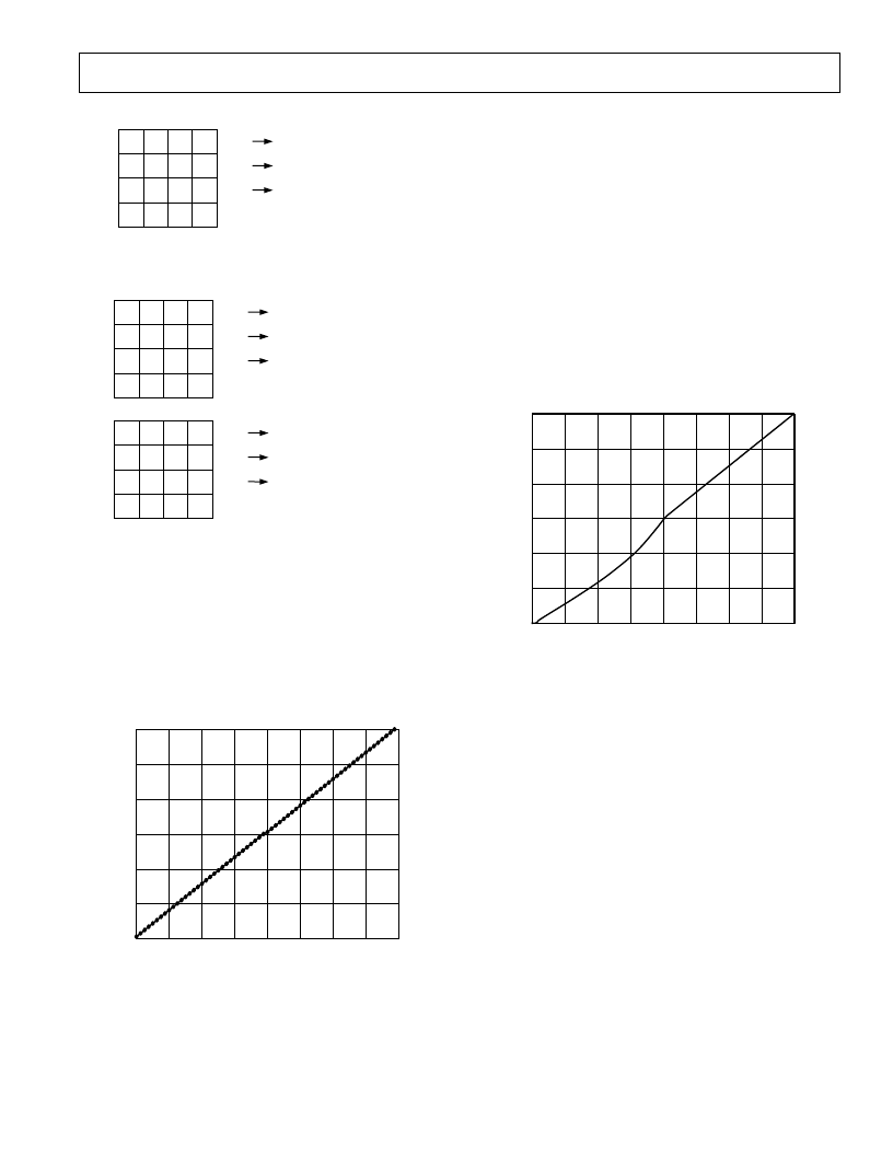
Variable Gain Amplifier
The VGA stage provides a gain range of 2 dB to 36 dB, program-
mable with 10-bit resolution through the serial digital interface.
Combined with 4 dB from the
PxGA
stage, the total gain range
for the AD984xA is 6 dB to 40 dB. The minimum gain of 6 dB
is needed to match a 1 V input signal with the ADC full-scale
range of 2 V. When compared to 1 V full-scale systems (such as
ADI’s AD9803), the equivalent gain range is 0 dB to 34 dB.
The VGA gain curve is divided into two separate regions. When
the VGA Gain Register code is between 0 and 511, the curve
follows a (1 + x)/(1 – x) shape, which is similar to a “linear-in-
dB” characteristic. From code 512 to code 1023, the curve follows
a “linear-in-dB” shape. The exact VGA gain can be calculated
for any Gain Register value by using the following two equations:
Code Range
Gain Equation (dB)
0–511
Gain
= 20 log
10
([658 +
code
]/[658 –
code
]) – 0.4
512 –1023
Gain
= (0.0354)(
code
) – 0.4
As shown in the CCD Mode Specifications, only the VGA gain
range from 2 dB to 36 dB has tested and guaranteed accuracy.
This corresponds to a VGA gain code range of 91 to 1023. The
Gain Accuracy Specifications also include the
PxGA
gain of 4 dB,
for a total gain range of 6 dB to 40 dB.
VGA GAIN REGISTER CODE
36
0
V
–
127
255
383
511
639
767
895
1023
30
24
18
12
6
0
Figure 29. VGA Gain Curve (Gain from PxGA Not Included)
Optical Black Clamp
The optical black clamp loop is used to remove residual offsets
in the signal chain, and to track low-frequency variations in the
CCD’s black level. During the optical black (shielded) pixel
interval on each line, the ADC output is compared with a fixed
black level reference, selected by the user in the Clamp Level
Register. Any value between 0 LSB and 64 LSB (AD9841A)
or 255 LSB (AD9842A) may be programmed, with 8-bit resolu-
tion. The resulting error signal is filtered to reduce noise, and
the correction value is applied to the ADC input through a
D/A converter. Normally, the optical black clamp loop is turned
on once per horizontal line, but this loop can be updated more
slowly to suit a particular application. If external digital clamping
is used during the post processing, the AD984xA’s optical black
clamping may be disabled using Bit D5 in the Operation Register
(see Serial Interface Timing and Internal Register Description
section). When the loop is disabled, the Clamp Level Register
may still be used to provide programmable offset adjustment.
Horizontal timing is shown in Figure 6. The CLPOB pulse
should be placed during the CCD’s optical black pixels. It is
recommended that the CLPOB pulse duration be at least 20
pixels wide to minimize clamp noise. Shorter pulsewidths may be
used, but clamp noise may increase, and the ability to track
low-frequency variations in the black level will be reduced.
相關PDF資料 |
PDF描述 |
|---|---|
| AD9842AJST | Complete 20 MSPS CCD Signal Processors |
| AD9843A | Complete 10-Bit 20 MSPS CCD Signal Processor |
| AD9843AJST | Complete 10-Bit 20 MSPS CCD Signal Processor |
| AD9844 | Complete 12-Bit 20 MSPS CCD Signal Processor |
| AD9844A | Complete 12-Bit 20 MSPS CCD Signal Processor |
相關代理商/技術參數 |
參數描述 |
|---|---|
| AD9841AJSTRL | 制造商:Analog Devices 功能描述:AFE Video 1ADC 10-Bit 3.3V 48-Pin LQFP T/R 制造商:Analog Devices 功能描述:AFE VID 1ADC 10-BIT 3.3V 48LQFP - Tape and Reel |
| AD9841AJSTZ | 功能描述:IC CCD SIGNAL PROC 10BIT 48LQFP RoHS:是 類別:集成電路 (IC) >> 接口 - 傳感器和探測器接口 系列:- 其它有關文件:Automotive Product Guide 產品培訓模塊:Lead (SnPb) Finish for COTS Obsolescence Mitigation Program 標準包裝:74 系列:- 類型:觸控式傳感器 輸入類型:數字 輸出類型:數字 接口:JTAG,串行 電流 - 電源:100µA 安裝類型:表面貼裝 封裝/外殼:20-TSSOP(0.173",4.40mm 寬) 供應商設備封裝:20-TSSOP 包裝:管件 |
| AD9841AJSTZRL | 功能描述:IC CCD SIGNAL PROC 10BIT 48LQFP RoHS:是 類別:集成電路 (IC) >> 接口 - 傳感器和探測器接口 系列:- 其它有關文件:Automotive Product Guide 產品培訓模塊:Lead (SnPb) Finish for COTS Obsolescence Mitigation Program 標準包裝:74 系列:- 類型:觸控式傳感器 輸入類型:數字 輸出類型:數字 接口:JTAG,串行 電流 - 電源:100µA 安裝類型:表面貼裝 封裝/外殼:20-TSSOP(0.173",4.40mm 寬) 供應商設備封裝:20-TSSOP 包裝:管件 |
| AD9841JST | 制造商:Rochester Electronics LLC 功能描述:- Tape and Reel |
| AD9841JSTRL | 制造商:Rochester Electronics LLC 功能描述:- Tape and Reel |
發布緊急采購,3分鐘左右您將得到回復。