- 您現在的位置:買賣IC網 > PDF目錄373970 > AD9875BST (ANALOG DEVICES INC) Broadband Modem Mixed-Signal Front End PDF資料下載
參數資料
| 型號: | AD9875BST |
| 廠商: | ANALOG DEVICES INC |
| 元件分類: | 通信及網絡 |
| 英文描述: | Broadband Modem Mixed-Signal Front End |
| 中文描述: | SPECIALTY TELECOM CIRCUIT, PQFP48 |
| 封裝: | LQFP-48 |
| 文件頁數: | 15/24頁 |
| 文件大小: | 288K |
| 代理商: | AD9875BST |
REV. 0
AD9875
–15–
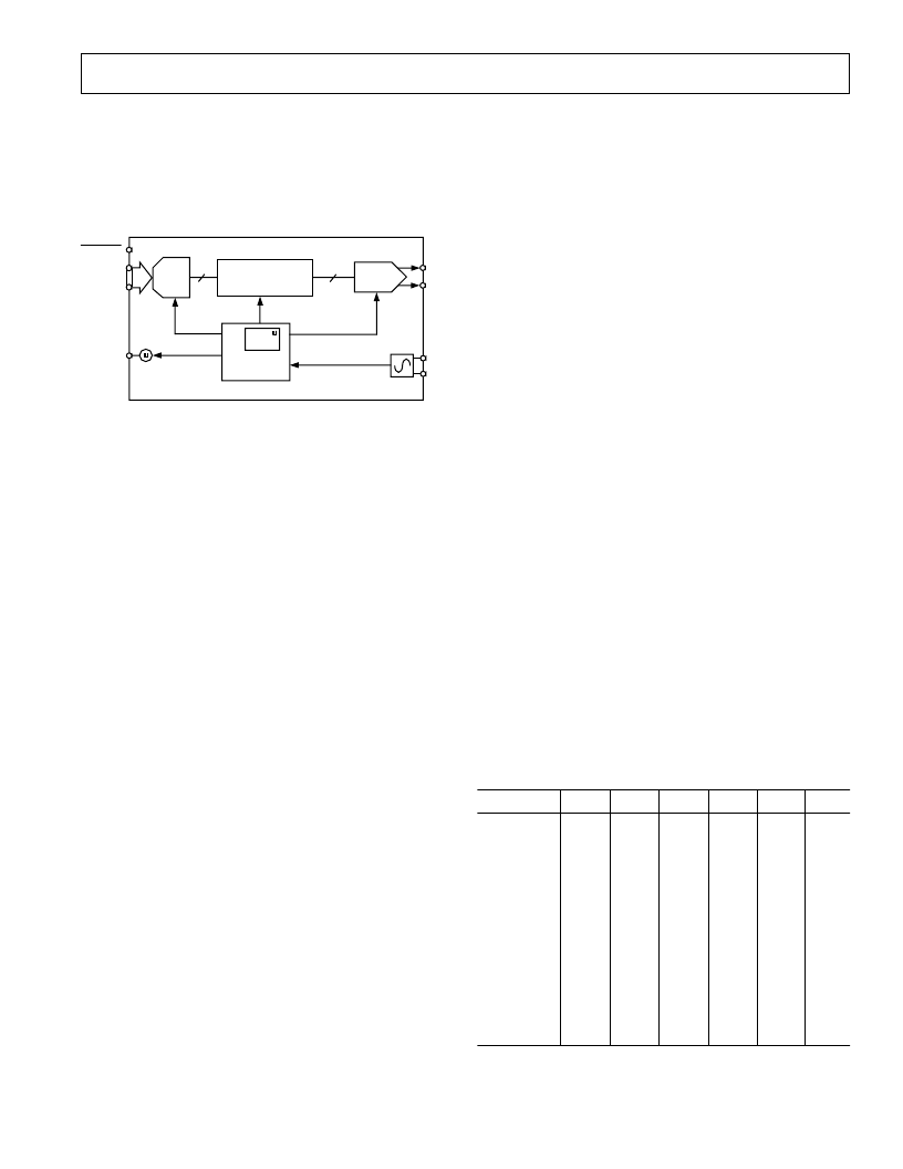
T RANSMIT PAT H
T he AD9875 transmit path consists of a Digital Interface Port,
a Programmable Interpolation Filter, and a T ransmit DAC. All
clock signals required by these blocks are generated from the
f
OSCIN
signal by the PLL-A clock generator. T he block diagram
below shows the interconnection between the major functional
components of the transmit path.
Tx+
Tx
–
OSCIN
XTAL
Kx INTERPOLATION
LPF/BPF
CLOCK GEN
PL L
Tx QUIET
GAIN
Tx [5:0]
Tx SYNC
CLK-A
f
CLK-A
f
DAC
= L
f
OSCIN
f
OSCIN
10
10
Tx
DEMUX
TxDAC+
AD9875
Figure 1
.
Transmit Path Block Diagram
DIGIT AL INT E RFACE PORT
T he transmit Digital Interface Port has several modes of
operation. In its default configuration, the T x Port accepts six
bit nibbles through the T x[5:0] and T xSY NC pins and demul-
tiplexes the data into 12-bit words before passing it to the
Interpolation Filter. T he input data is sampled on the rising
edge of f
CLK -A
.
Additional programming options for the T x Port allow; sampling
the input data on the falling edge of f
CLK –A
, inversion or dis-
abling of f
CLK -A
, reversing the order of the nibbles, and inputting
nibble widths of 5 bits/5 bits. Also, the T x Port interface can be
controlled by the GAIN pin to provide direct access to the Rx
Path Gain Adjust register. All of these modes are fully described
in the Register Programming Definitions section of this data sheet.
T he data format is two’s complement, as shown below:
011 . . 11: Maximum
000 . . 01: Midscale + 1 LSB
000 . . 00: Midscale
111 . . 11: Midscale – 1 LSB
111 . . 10: Midscale – 2 LSB
100 . . 00: Minimum
T he data can be translated to straight binary data format by
simply inverting the most significant bit.
T he timing of the interface is fully described in the T ransmit
T iming section of this data sheet.
PLL-A CLOCK DIST RIBUT ION
Figure 1 shows the clock signals used in the transmit path. T he
DAC sampling clock, f
DAC
, is generated by DPLL-A. f
DAC
has a
frequency equal to L
×
f
OSCIN
, where f
OSCIN
is the internal signal
generated either by the crystal oscillator when a crystal is con-
nected between the OSCIN and X T AL pins, or by the clock that
is fed into the OSCIN pin, and L is the multiplier programmed
through the serial port. L can have the values of 1, 2, 4, or 8.
T he transmit path expects a new half-word of data at the rate
of f
CLK -A
. When the T x multiplexer is enabled, the frequency
of the T x port is:
f
CLK-A
= 2
×
f
DAC
/K
= 2
×
L
×
f
OSCIN
/K
where
K
is the interpolation factor that can be programmed to
be 1, 2, or 4.
When the T x multiplexer is disabled, the frequency of the T x port is:
f
CLK-A
=
f
DAC
/K
=
L
×
f
OSCIN
/K
.
INT E RPOLAT ION FILT E R
T he interpolation filter can be programmed to run at 2
×
and 4
×
upsampling ratios in each of three different modes. T he transfer
functions of these six configurations are shown in T PCs 1–6.
T he X -axis of each of these figures corresponds to the frequency
normalized to f
DAC
. T hese transfer functions show both the
discrete time transfer function of the interpolation filters alone
and with the SIN(x)/x transfer function of the DAC. T he Inter-
polation Filter can also be programmed into a pass-through mode
if no interpolation filtering is desired.
T he contents of the interpolation filters are not cleared by
hardware or software resets. It is recommended to “flush” the
transmit data path with zeros before transmitting data.
T able I contains the following parameters as a function of the
mode that it is programmed:
Latency
– the number of clock cycles from the time a digital
impulse is written to the DAC until the peak value is output at
the T x
±
pins.
Flush
– the number of clock cycles from the time a digital
impulse is written to the DAC until the output at the T x
±
pins
settles to zero.
f
LOWER
(0.1 dB, 3 dB)
– T his indicates the lower 0.1 dB or 3 dB
cutoff frequency of the interpolation filter as a fraction of f
DAC
,
the DAC sampling frequency.
f
UPPER
(0.1 dB, 3 dB)
– T his indicates the upper 0.1 dB or 3 dB
cutoff frequency of the interpolation filter as a fraction of f
DAC
,
the DAC sampling frequency.
T able I. Interpolation Filter Parameters vs. Mode
Register 7[7:4]
0
0
0
1
0
4
0
5
0
8
0
C
Mode
4
×
LPF 2
×
LPF 4
×
BPF 2
×
BPF 4
×
BPF 4
×
BPF
Adj.
86
30
86
Adj.
30
Lower
86
Upper
86
Latency, f
DAC
Clock Cycles
Flush, f
DAC
Clock Cycles
f
LOWER,
0.1 dB
128
48
128
48
142
142
0
0
0.398
0.276
0.148/
0.774
0.226/
0.852
0.131/
0.757
0.243/
0.869
0.274/
0.648
0.352/
0.762
0.257/
0.631
0.369/
0.743
f
UPPER,
0.1 dB
0.102
0.204
0.602
0.724
f
LOWER,
3 dB
0
0
0.381
0.262
f
UPPER,
3 dB
0.119
0.238
0.619
0.738
相關PDF資料 |
PDF描述 |
|---|---|
| AD9876 | Broadband Modem Mixed-Signal Front End |
| AD9876-EB | Broadband Modem Mixed-Signal Front End |
| AD9876BST | Broadband Modem Mixed-Signal Front End |
| AD9876BSTRL | Broadband Modem Mixed-Signal Front End |
| AD9877 | Mixed-Signal Front End Set-Top Box, Cable Modem |
相關代理商/技術參數 |
參數描述 |
|---|---|
| AD9875BSTRL | 制造商:Analog Devices 功能描述:Modem Chip Single 48-Pin LQFP T/R |
| AD9875BSTZ | 制造商:Analog Devices 功能描述:Modem Chip Single 48-Pin LQFP |
| AD9875-EB | 制造商:Analog Devices 功能描述: |
| AD9876 | 制造商:AD 制造商全稱:Analog Devices 功能描述:Broadband Modem Mixed-Signal Front End |
| AD9876ABST | 制造商:Rochester Electronics LLC 功能描述:12B BROADBAND MODEM MXFE CONVERTER - Tape and Reel 制造商:Analog Devices 功能描述: |
發布緊急采購,3分鐘左右您將得到回復。