- 您現在的位置:買賣IC網 > PDF目錄373970 > AD9875BSTRL (ANALOG DEVICES INC) Broadband Modem Mixed-Signal Front End PDF資料下載
參數資料
| 型號: | AD9875BSTRL |
| 廠商: | ANALOG DEVICES INC |
| 元件分類: | 通信及網絡 |
| 英文描述: | Broadband Modem Mixed-Signal Front End |
| 中文描述: | SPECIALTY TELECOM CIRCUIT, PQFP48 |
| 封裝: | LQFP-48 |
| 文件頁數: | 19/24頁 |
| 文件大小: | 288K |
| 代理商: | AD9875BSTRL |
REV. 0
AD9875
–19–
Bits I4:I0 – A4:A0
T hese bits determine which register is accessed during the data
transfer portion of the communications cycle. For multibyte
transfers, this address is the starting byte address. T he remain-
ing register addresses are generated by the AD9875.
Serial Interface Port Pin Description
SCLK—Serial Clock
T he serial clock pin is used to synchronize data transfers to and
from the AD9875 and to run the internal state machines. SCLK
maximum frequency is 25 MHz. All data transmitted to the
AD9875 is sampled on the rising edge of SCLK . All data read
from the AD9875 is validated on the rising edge of SCLK and is
updated on the falling edge.
SENABLE
—Serial Interface E nable
T he
SENABLE
pin is active low. It enables the serial communi-
cation to the device.
SENABLE
select should stay low during
the entire communication cycle. All input on the serial port is
ignored when
SENABLE
is inactive.
SDAT A—Serial Data I/O
T he signal on this line is sampled on the first eight rising edges
of SCLK after
SENABLE
goes active. Data is then read from or
written to the AD9875 depending on what was read.
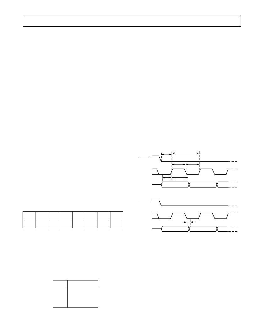
Figures 8 and 9 show the timing relationships between the three
SPI signals.
SENABLE
SCLK
SDATA
t
DH
t
DS
t
DS
t
PWH
t
SCLK
t
PWL
INSTRUCTION BIT 7
INSTRUCTION BIT 6
Figure 8. Timing Diagram Register Write to AD9875/AD9876
SENABLE
SCLK
SDATA
DATA BIT n
DATA BIT n
–
1
t
DV
Figure 9. Timing Diagram Register Read from AD9875/AD9876
MSB/LSB T ransfers
T he AD9875 serial port can support both most significant bit
(MSB) first or least significant bit (LSB) first data formats. T he
bit order is controlled by the
SPI LSB First
bit (Register 0, Bit 6).
T he default is value is 0, MSB first. Multibyte data transfers in
MSB format can be completed by writing an instruction byte
that includes the register address of the last address to be accessed.
T he AD9875 will automatically decrement the address for each
successive byte required for the multibyte communication cycle.
When the
SPI LSB First
bit (Register 0, Bit 6) is set high, the
serial port interprets both instruction and data bytes LSB first.
Multibyte data transfers in LSB format can be completed by
writing an instruction byte that includes the register address of
the first address to be accessed. T he AD9875 will automatically
increment the address for each successive byte required for the
multibyte communication cycle.
For the AD9875, the most significant nibble defaults to six bits
and the least significant nibble defaults to four bits. T his can be
changed so that the least significant nibble and most significant
nibble have five bits each. T his is done by setting the
Rx Port
Width Five Bits
bit (Register 8, Bit 1). In all cases, the nibbles
are justified toward Bit 5.
Also, the Rx path can be used in a reduced resolution mode by
setting the
Rx Port Multiplexer Bypass
bit (Register 8, Bit 0). In
this mode the Rx data word becomes six bits and is read in a
single cycle. T he clocking modes are the same as described above,
but the level of Rx SYNC will stay low.
T he Rx[5:0] pins can be put into a high impedance state by
setting the
Three-State Rx Port
bit (Register 8, Bit 3).
SE RIAL INT E RFACE FOR RE GIST E R CONT ROL
T he serial port is a three wire serial communications port consisting
of a clock (SCLK ), chip select (
SENABLE
), and a bidirectional
data (SDAT A) signal. T he interface allows read/write access to
all registers that configure the AD9875 internal parameters.
Single or multiple byte transfers are supported as well as MSB
first or LSB first transfer formats.
General Operation of the Serial Interface
Serial communication over the serial interface can be from 1 to
5 bytes in length. T he first byte is always the instruction byte.
T he instruction byte establishes whether the communication is
going to be a read or write access, the number of data bytes to
be transferred and the address of the first register to be accessed.
T he instruction byte transfer is complete immediately upon the
eighth rising edge of SCLK after
SENABLE
is asserted. Like-
wise, the data registers change
immediately
upon writing to the
eighth bit of each data byte.
Instruction Byte
T he instruction byte contains the following information as
shown below:
T able II. Instruction Byte Information
B
S
M
B
S
L
7
I
6
I
5
I
4
I
3
I
2
I
1
I
0
I
W
/
R
1
N
0
N
4
A
3
A
2
A
1
A
0
A
Bit I7 – R/W
T his bit determines whether a read or a write data transfer will
occur after the instruction byte write. Logic high indicates read
operation; logic zero indicates a write operation.
Bits I6:I5 – N1:N0
T hese two bits determine the number of bytes to be transferred
during the data transfer cycle. T he bit decodes are shown in the
table below:
T able III. Decode Bits
N1:N0
Description
0:0
0:1
1:0
1:1
T ransfer 1 Byte
T ransfer 2 Bytes
T ransfer 3 Bytes
T ransfer 4 Bytes
相關PDF資料 |
PDF描述 |
|---|---|
| AD9875 | Broadband Modem Mixed-Signal Front End |
| AD9875-EB | Broadband Modem Mixed-Signal Front End |
| AD9875BST | Broadband Modem Mixed-Signal Front End |
| AD9876 | Broadband Modem Mixed-Signal Front End |
| AD9876-EB | Broadband Modem Mixed-Signal Front End |
相關代理商/技術參數 |
參數描述 |
|---|---|
| AD9875BSTZ | 制造商:Analog Devices 功能描述:Modem Chip Single 48-Pin LQFP |
| AD9875-EB | 制造商:Analog Devices 功能描述: |
| AD9876 | 制造商:AD 制造商全稱:Analog Devices 功能描述:Broadband Modem Mixed-Signal Front End |
| AD9876ABST | 制造商:Rochester Electronics LLC 功能描述:12B BROADBAND MODEM MXFE CONVERTER - Tape and Reel 制造商:Analog Devices 功能描述: |
| AD9876ABSTRL | 制造商:Rochester Electronics LLC 功能描述:12B BROADBAND MODEM MXFE CONVERTER - Tape and Reel 制造商:Analog Devices 功能描述: |
發布緊急采購,3分鐘左右您將得到回復。