- 您現在的位置:買賣IC網 > PDF目錄373971 > AD9944KCP (ANALOG DEVICES INC) Complete 10-Bit and 12-Bit, 25 MHz CCD Signal Processors PDF資料下載
參數資料
| 型號: | AD9944KCP |
| 廠商: | ANALOG DEVICES INC |
| 元件分類: | 消費家電 |
| 英文描述: | Complete 10-Bit and 12-Bit, 25 MHz CCD Signal Processors |
| 中文描述: | SPECIALTY CONSUMER CIRCUIT, QCC32 |
| 封裝: | 5 X 5 MM, MO-220-VHHD-2, LFCSP-32 |
| 文件頁數: | 15/20頁 |
| 文件大小: | 485K |
| 代理商: | AD9944KCP |
AD9943/AD9944
CIRCUIT DESCRIPTION AND OPERATION
Rev. B | Page 15 of 20
6dB TO 40dB
CCDIN
DIGITAL
FILTERING
CLPOB
DC RESTORE
OPTICAL BLACK
CLAMP
DOUT
10-/12-BIT
ADC
VGA
8-BIT
DAC
CLAMP LEVEL
REGISTER
8
VGA GAIN
REGISTER
10
CDS
INTERNAL
V
REF
2V FULL SCALE
10/12
0.1
μ
F
0
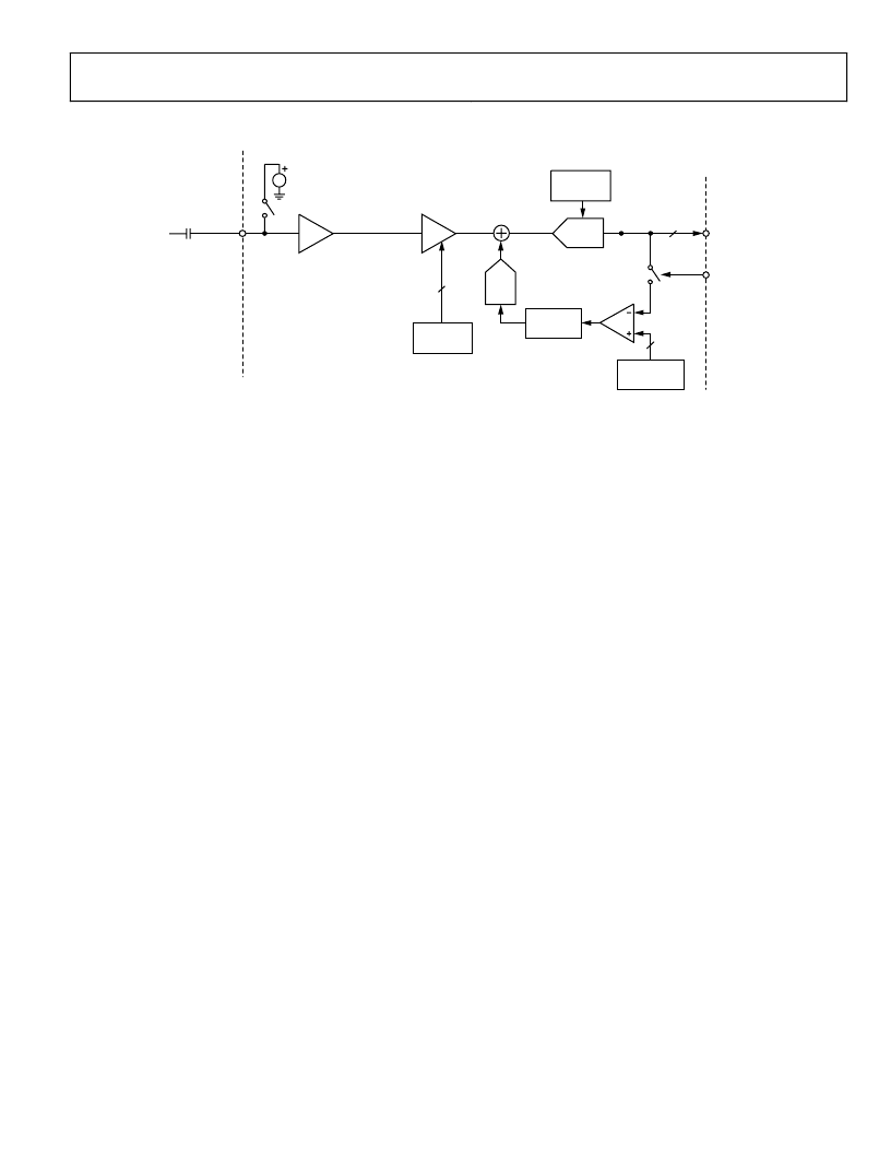
Figure 12. CCD Mode Block Diagram
The AD9943/AD9944 signal processing chain is shown in
Figure 12. Each processing step is essential for achieving a high
quality image from the raw CCD pixel data.
DC RESTORE
To reduce the large dc offset of the CCD output signal, a dc
restore circuit is used with an external 0.1 μF series coupling
capacitor. This restores the dc level of the CCD signal to
approximately 1.5 V, which is compatible with the 3 V single
supply of the AD9943/AD9944.
CORRELATED DOUBLE SAMPLER
The CDS circuit samples each CCD pixel twice to extract video
information and reject low frequency noise. The timing shown
in Figure 14 illustrates how the two CDS clocks, SHP and SHD,
are used, respectively, to sample the reference level and data
level of the CCD signal. The CCD signal is sampled on the
rising edges of SHP and SHD. Placement of these two clock
signals is critical for achieving the best performance from the
CCD. An internal SHP/SHD delay (t
ID
) of 3 ns is caused by
internal propagation delays.
OPTICAL BLACK CLAMP
The optical black clamp loop is used to remove residual offsets
in the signal chain and to track low frequency variations in the
CCD’s black level. During the optical black (shielded) pixel
interval on each line, the ADC output is compared with the
fixed black level reference selected by the user in the clamp level
register. The resulting error signal is filtered to reduce noise, and
the correction value is applied to the ADC input through a D/A
converter. Normally, the optical black clamp loop is turned on
once per horizontal line, but this loop can be updated more
slowly to suit a particular application. If external digital
clamping is used during the post processing, the optical black
clamping for the AD9943/AD9944 may be disabled using
Bit D3 in the operation register. Refer to Table 9 and Figure 10
and Figure 11.
When the loop is disabled, the clamp level register may still be
used to provide programmable offset adjustment. Horizontal
timing is shown in Figure 15. The CLPOB pulse should be
placed during the CCD’s optical black pixels. It is recommended
that the CLPOB pulse be used during valid CCD dark pixels.
The CLPOB pulse should be a minimum of 20 pixels wide to
minimize clamp noise. Shorter pulse widths may be used, but
clamp noise may increase and the loop’s ability to track low
frequency variations in the black level is reduced.
相關PDF資料 |
PDF描述 |
|---|---|
| AD9944KCPRL | Complete 10-Bit and 12-Bit, 25 MHz CCD Signal Processors |
| AD9944KCPZ | Complete 10-Bit and 12-Bit, 25 MHz CCD Signal Processors |
| AD9944KCPZRL | Complete 10-Bit and 12-Bit, 25 MHz CCD Signal Processors |
| AD9943KCP | Complete 10-Bit and 12-Bit, 25 MHz CCD Signal Processors |
| AD9943KCPRL | Complete 10-Bit and 12-Bit, 25 MHz CCD Signal Processors |
相關代理商/技術參數 |
參數描述 |
|---|---|
| AD9944KCPRL | 制造商:Analog Devices 功能描述:AFE Video 1ADC 12-Bit 3V 32-Pin LFCSP EP T/R 制造商:Rochester Electronics LLC 功能描述:- Tape and Reel |
| AD9944KCPZ | 功能描述:IC CCD SIGNAL PROCESSOR 32-LFCSP RoHS:是 類別:集成電路 (IC) >> 接口 - 傳感器和探測器接口 系列:- 其它有關文件:Automotive Product Guide 產品培訓模塊:Lead (SnPb) Finish for COTS Obsolescence Mitigation Program 標準包裝:74 系列:- 類型:觸控式傳感器 輸入類型:數字 輸出類型:數字 接口:JTAG,串行 電流 - 電源:100µA 安裝類型:表面貼裝 封裝/外殼:20-TSSOP(0.173",4.40mm 寬) 供應商設備封裝:20-TSSOP 包裝:管件 |
| AD9944KCPZ1 | 制造商:AD 制造商全稱:Analog Devices 功能描述:Complete 10-Bit and 12-Bit, 25 MHz CCD Signal Processors |
| AD9944KCPZRL | 功能描述:IC CCD SIGNAL PROCESSOR 32-LFCSP RoHS:是 類別:集成電路 (IC) >> 接口 - 傳感器和探測器接口 系列:- 其它有關文件:Automotive Product Guide 產品培訓模塊:Lead (SnPb) Finish for COTS Obsolescence Mitigation Program 標準包裝:74 系列:- 類型:觸控式傳感器 輸入類型:數字 輸出類型:數字 接口:JTAG,串行 電流 - 電源:100µA 安裝類型:表面貼裝 封裝/外殼:20-TSSOP(0.173",4.40mm 寬) 供應商設備封裝:20-TSSOP 包裝:管件 |
| AD9944KCPZRL1 | 制造商:AD 制造商全稱:Analog Devices 功能描述:Complete 10-Bit and 12-Bit, 25 MHz CCD Signal Processors |
發布緊急采購,3分鐘左右您將得到回復。