- 您現在的位置:買賣IC網 > PDF目錄373972 > AD9958 (Analog Devices, Inc.) 2-Channel 500 MSPS DDS with 10-Bit DACs PDF資料下載
參數資料
| 型號: | AD9958 |
| 廠商: | Analog Devices, Inc. |
| 英文描述: | 2-Channel 500 MSPS DDS with 10-Bit DACs |
| 中文描述: | 雙通道500 MSPS的DDS的10位DAC |
| 文件頁數: | 22/40頁 |
| 文件大小: | 1051K |
| 代理商: | AD9958 |
第1頁第2頁第3頁第4頁第5頁第6頁第7頁第8頁第9頁第10頁第11頁第12頁第13頁第14頁第15頁第16頁第17頁第18頁第19頁第20頁第21頁當前第22頁第23頁第24頁第25頁第26頁第27頁第28頁第29頁第30頁第31頁第32頁第33頁第34頁第35頁第36頁第37頁第38頁第39頁第40頁
AD9958
2-Level Modulation Using Profile Pins for RU/RD
When the RU/RD bit = 01, Profile Pins P2 and P3 are available
for RU/RD. Note that only a modulation level of two is available
in this mode. See Table 13 for available pin assignments.
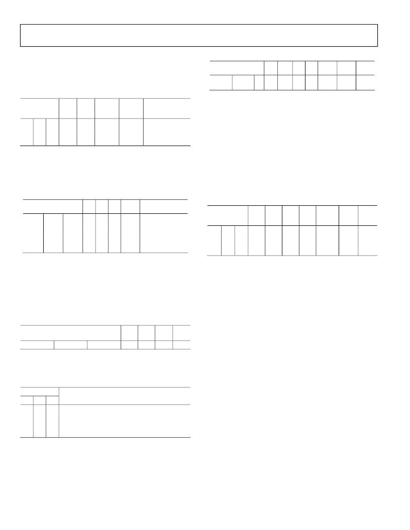
Table 13.
Profile Pin
Config. Bits
FR1 <14:12>
P0
P1
P2
1
0
1
CH0
CH1
CH0
Rev. 0 | Page 22 of 40
P3
CH1
Description
2-level
modulation
With RU/RD, CH0,
CH1
RU/RD
RU/RD
8-Level Modulation Using a Profile Pin for RU/RD
When the RU/RD bit = 10, Profile Pin P3 is available for
RU/RD. Note that only a modulation level of eight is available.
See Table 14 for available pin assignments.
Table 14.
Profile Pin Config. Bits
FR1 <14:12>
P0
P1
x
1
0
CH0 CH0 CH0 CH0
P2
P3
Description
8-level modulation
with RU/RD,
CH0
8-level modulation
with RU/RD,
CH1
RU/RD
x
1
1
CH1 CH1 CH1 CH1
RU/RD
MODULATION USING SDIO PINS FOR RU/RD
For RU/RD bits = 11, SDIO Pins 1, 2, and 3 are available for
RU/RD. In this mode, modulation levels of 2/4/16 are available.
Note that the serial I/O port can only be used in 1-bit serial
mode.
2-Level Modulation Using SDIO Pins for RU/RD
Table 15.
Profile Pin Config. Bits
FR1 <14:12>
x
x
x
P0
N/A
P1
N/A CH0
P2
P3
CH1
For this configuration, each profile pin is dedicated to a specific
channel. In this case, the SDIO pins can be used for the RU/RD
function, as described in Table 16.
Table 16.
SDIO Pins
1
2
3
Description
1
0
0
Triggers the ramp-up function for CH0
1
0
1
Triggers the ramp-down function for CH0
1
1
0
Triggers the ramp-up function for CH1
1
1
1
Triggers the ramp-down function for CH1
4-Level Modulation Using SDIO Pins for RU/RD
For RU/RD = 11 (SDIO Pins 1 and 2 are available for RU/RD),
the modulation level is set to four. See Table 17 for pin
assignments, including SDIO pin assignments.
Table 17.
Profile Pin Config.
Bits FR1 <14:12>
1
P0
CH0 CH0 CH1 CH1 CH0
P1
P2
P3
SDIO 1 SDIO 2 SDIO 3
CH1
RU/RD RU/RD
0
1
N/A
For the configuration shown in Table 17, the profile register is
chosen based on the two bit value presented to <P1:P2> or
<P3:P4>.
For example, if PPC = 101, <P0:P1> = 11, and <P2:P3> = 01,
then the contents of Profile Register 3 of Channel 0 are
presented to Channel 0’s output and the contents of Profile
Register 1 of Channel 1 are presented to Channel 1’s output.
SDIO Pins 1 and 2 provide the RU/RD function.
16-Level Modulation Using SDIO Pins for RU/RD
RU/RD = 11 (SDIO Pin 1 available for RU/RD) and the level is
set to 16. See the pin assignment shown in the Table 18.
Table 18.
Profile Pin
Configuration
FR1<14:12>
P0
P1
P2
x
1
0
CH0
CH0
CH0
x
1
1
CH1
CH1
CH1
P3
CH0
CH1
SDIO
1
CH0
RU/RD
CH1
RU/RD
SDIO
2
NA
NA
SDIO
3
NA
NA
For the configuration shown in Table 18, the profile register is
chosen based on the 4-bit value presented to <P0:P3>. For
example, if PPC = X11 and <P0-P3> = 1101, then the contents
of Profile Register 13 of Channel 1 is presented to Channel 1.
The SDIO_1 pin provides the RU/RD function.
LINEAR SWEEP (SHAPED) MODULATION MODE
Linear sweep enables the user to sweep frequency, phase, or
amplitude from a starting point (S0) to an endpoint (E0). The
purpose of linear sweep modes is to provide better bandwidth
containment compared to direct modulation by replacing
greater instantaneous changes with more gradual, user-defined
changes between S0 and E0.
In linear sweep mode, S0 is loaded into Profile Register 0
(Profile 0 is represented by one of the three Registers 0x04,
0x05, or 0x06 depending on the type of sweep) and E0 is always
loaded into Profile Register 1 (Register 0x0A). If E0 is
configured for frequency sweep, the resolution is 32 bits, phase
sweep is 14 bits, and amplitude sweep is 10 bits. When sweeping
phase or amplitude, the word value must be MSB-aligned in
Profile 1 register. The unused bits are don’t care bits.
The profile pins are used to trigger and control the direction of
the linear sweep for frequency, phase, and amplitude. Both
channels can be programmed separately for a linear sweep. In
linear sweep mode, Profile Pin 2 is dedicated to Channel 0.
Profile Pin 3 is dedicated to Channel 1, and so on.
相關PDF資料 |
PDF描述 |
|---|---|
| AD9958BCPZ | 2-Channel 500 MSPS DDS with 10-Bit DACs |
| AD9970 | 14-Bit CCD Signal Processor with Precision Timing Generator |
| AD9971 | 12-Bit CCD Signal Processor with Precision Timing |
| AD9973 | Dual-Channel, 14-Bit CCD Signal Processor with Precision Timing⑩ Core |
| AD9974 | Dual-Channel, 14-Bit, CCD Signal Processor with Precision Timing⑩ Core |
相關代理商/技術參數 |
參數描述 |
|---|---|
| AD9958 PCB | 制造商:Analog Devices 功能描述:EVAL BOARD ((NS)) |
| AD9958/PCB | 制造商:Analog Devices 功能描述:Evaluation Board For 2-Channel 500 MSPS DDS With 10-Bit DACs 制造商:Rochester Electronics LLC 功能描述:- Bulk 制造商:Analog Devices 功能描述:IC 10-BIT DAC DDS |
| AD9958/PCBZ | 功能描述:BOARD EVALUATION FOR AD9958 RoHS:是 類別:編程器,開發系統 >> 評估演示板和套件 系列:AgileRF™ 標準包裝:1 系列:PSoC® 主要目的:電源管理,熱管理 嵌入式:- 已用 IC / 零件:- 主要屬性:- 次要屬性:- 已供物品:板,CD,電源 |
| AD9958/PCBZ | 制造商:Analog Devices 功能描述:EVAL BOARD, AD9958 DIRECT DIGITAL SYNTHE |
| AD9958_08 | 制造商:AD 制造商全稱:Analog Devices 功能描述:2-Channel, 500 MSPS DDS with 10-Bit DACs |
發布緊急采購,3分鐘左右您將得到回復。