- 您現(xiàn)在的位置:買賣IC網(wǎng) > PDF目錄373973 > ADA4841-1 (Analog Devices, Inc.) Low Power, Low Noise and Distortion, Rail-to-Rail Output Amplifier PDF資料下載
參數(shù)資料
| 型號(hào): | ADA4841-1 |
| 廠商: | Analog Devices, Inc. |
| 英文描述: | Low Power, Low Noise and Distortion, Rail-to-Rail Output Amplifier |
| 中文描述: | 低功耗,低噪聲和失真,軌到軌輸出放大器 |
| 文件頁(yè)數(shù): | 6/20頁(yè) |
| 文件大小: | 442K |
| 代理商: | ADA4841-1 |
第1頁(yè)第2頁(yè)第3頁(yè)第4頁(yè)第5頁(yè)當(dāng)前第6頁(yè)第7頁(yè)第8頁(yè)第9頁(yè)第10頁(yè)第11頁(yè)第12頁(yè)第13頁(yè)第14頁(yè)第15頁(yè)第16頁(yè)第17頁(yè)第18頁(yè)第19頁(yè)第20頁(yè)
ADA4841-1/ADA4841-2
ABSOLUTE MAXIMUM RATINGS
Table 4.
Parameter
Supply Voltage
Power Dissipation
Common-Mode Input Voltage
Differential Input Voltage
Storage Temperature Range
Operating Temperature Range
Lead Temperature
Junction Temperature
Rev. C | Page 6 of 20
Rating
12.6 V
See Figure 5
V
S
0.5 V to +V
S
+ 0.5 V
±
1.8 V
65°C to +125°C
40°C to +85°C
JEDEC J-STD-20
150°C
Stresses above those listed under Absolute Maximum Ratings
may cause permanent damage to the device. This is a stress
rating only; functional operation of the device at these or any
other conditions above those indicated in the operational
section of this specification is not implied. Exposure to absolute
maximum rating conditions for extended periods may affect
device reliability.
THERMAL RESISTANCE
θ
JA
is specified for the worst-case conditions, that is, θ
JA
is
specified for device soldered in circuit board for surface-mount
packages.
Table 5. Thermal Resistance
Package Type
8-lead SOIC_N
8-lead MSOP
6-Lead SOT-23
Maximum Power Dissipation
The maximum safe power dissipation for the ADA4841-1/
ADA4841-2 is limited by the associated rise in junction
temperature (T
J
) on the die. At approximately 150
°
C, which is
the glass transition temperature, the plastic changes its
properties. Even temporarily exceeding this temperature limit
may change the stresses that the package exerts on the die,
permanently shifting the parametric performance of the
amplifiers. Exceeding a junction temperature of 150°C for an
extended period can result in changes in silicon devices,
potentially causing degradation or loss of functionality.
θ
JA
125
130
170
Unit
°C/W
°C/W
°C/W
The power dissipated in the package (P
D
) is the sum of the
quiescent power dissipation and the power dissipated in the die
due to the amplifier’s drive at the output. The quiescent power is
the voltage between the supply pins (V
S
) times the quiescent
current (I
S
).
P
D
=
Quiescent Power
+ (
Total Drive Power
Load Power
)
(
)
L
OUT
R
L
OUT
R
S
S
S
D
V
V
V
2
I
V
P
2
×
+
×
=
RMS output voltages should be considered. If R
L
is referenced
to V
S
, as in single-supply operation, the total drive power is
V
S
× I
OUT
. If the rms signal levels are indeterminate, consider the
worst case, when V
OUT
= V
S
/4 for R
L
to midsupply.
(
)
S
S
S
D
R
(
)
L
V
I
V
P
2
4
+
×
=
In single-supply operation with R
L
referenced to V
S
, worst case
is V
OUT
= V
S
/2.
Airflow increases heat dissipation, effectively reducing θ
JA
.
In addition, more metal directly in contact with the package
leads and through holes under the device reduces θ
JA
.
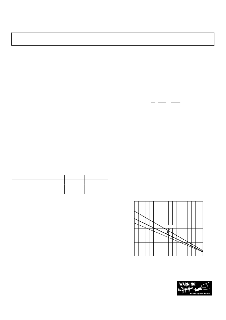
Figure 5 shows the maximum safe power dissipation in the
package vs. the ambient temperature for the 8-lead MSOP
(145°C/W), 8-lead SOIC_N (125°C/W) and the 6-lead SOT-23
(170°C/W) on a JEDEC standard 4-layer board. θ
JA
values are
approximations.
2.0
0
–55
125
0
AMBIENT TEMPERATURE (°C)
M
1.5
1.0
0.5
–45 –35 –25 –15 –5
5
15 25 35 45 55 65 75 85 95 105 115
SOT-23
SOIC
MSOP
Figure 5. Maximum Power Dissipation vs. Temperature for a 4-Layer Board
ESD CAUTION
ESD (electrostatic discharge) sensitive device. Electrostatic charges as high as 4000 V readily accumulate on
the human body and test equipment and can discharge without detection. Although this product features
proprietary ESD protection circuitry, permanent damage may occur on devices subjected to high energy
electrostatic discharges. Therefore, proper ESD precautions are recommended to avoid performance
degradation or loss of functionality.
相關(guān)PDF資料 |
PDF描述 |
|---|---|
| ADA4841-1YRJZ-R2 | Low Power, Low Noise and Distortion, Rail-to-Rail Output Amplifier |
| ADA4841-1YRJZ-R7 | Low Power, Low Noise and Distortion, Rail-to-Rail Output Amplifier |
| ADA4841-1YRJZ-RL | Low Power, Low Noise and Distortion, Rail-to-Rail Output Amplifier |
| ADA4841-1YRZ | Low Power, Low Noise and Distortion, Rail-to-Rail Output Amplifier |
| ADA4841-1YRZ-R7 | Low Power, Low Noise and Distortion, Rail-to-Rail Output Amplifier |
相關(guān)代理商/技術(shù)參數(shù) |
參數(shù)描述 |
|---|---|
| ADA4841-1YR-EBZ | 制造商:AD 制造商全稱:Analog Devices 功能描述:Low Power, Low Noise and Distortion ail-to-Rail Output Amplifiers |
| ADA4841-1YRJ-EBZ | 功能描述:BOARD EVAL FOR ADA4841-1YRJ RoHS:是 類別:編程器,開(kāi)發(fā)系統(tǒng) >> 評(píng)估板 - 運(yùn)算放大器 系列:- 產(chǎn)品培訓(xùn)模塊:Lead (SnPb) Finish for COTS Obsolescence Mitigation Program 標(biāo)準(zhǔn)包裝:1 系列:- |
| ADA4841-1YRJZ | 制造商:Analog Devices 功能描述:OP AMP VF R-R LP LN SOT23-6 制造商:Analog Devices 功能描述:OP AMP, VF, R-R, LP, LN, SOT23-6 制造商:Analog Devices 功能描述:OP AMP, VF, R-R, LP, LN, SOT23-6, Op Amp Type:Rail to Rail, No. of Amplifiers:1, 制造商:Analog Devices 功能描述:OP AMP, VF, R-R, LP, LN, SOT23-6, Op Amp Type:Rail to Rail, No. of Amplifiers:1, Slew Rate:13V/s, Supply Voltage Range:2.7V to 12V, Amplifier Case Style:SOT-23, No. of Pins:6, Bandwidth:80MHz, Operating Temperature Min:-40C, , RoHS Compliant: Yes |
| ADA4841-1YRJZ-R2 | 制造商:Analog Devices 功能描述:OP Amp Single Volt Fdbk R-R O/P ±6V/12V 6-Pin SOT-23 T/R 制造商:Analog Devices 功能描述:OP AMP SGL VOLT FDBK R-R O/P 6V/12V 6PIN SOT-23 - Tape and Reel 制造商:Rochester Electronics LLC 功能描述: 制造商:Analog Devices 功能描述:IC OP AMPVFR-RLPLNSOT23-6 制造商:Analog Devices 功能描述:IC, OP-AMP, 80MHZ, 13V/ us, SOT-23-6, Op Amp Type:Low Power, No. of Amplifiers:1 |
| ADA4841-1YRJZ-R2 | 制造商:Analog Devices 功能描述:IC OP-AMP 80MHZ 13V/S SOT-23-6 |
發(fā)布緊急采購(gòu),3分鐘左右您將得到回復(fù)。