- 您現在的位置:買賣IC網 > PDF目錄373974 > ADA4841-1YRZ-R7 (ANALOG DEVICES INC) Low Power, Low Noise and Distortion, Rail-to-Rail Output Amplifier PDF資料下載
參數資料
| 型號: | ADA4841-1YRZ-R7 |
| 廠商: | ANALOG DEVICES INC |
| 元件分類: | 運動控制電子 |
| 英文描述: | Low Power, Low Noise and Distortion, Rail-to-Rail Output Amplifier |
| 中文描述: | OP-AMP, 300 uV OFFSET-MAX, PDSO8 |
| 封裝: | ROHS COMPLIANT, MS-012AA, SOIC-8 |
| 文件頁數: | 15/20頁 |
| 文件大小: | 442K |
| 代理商: | ADA4841-1YRZ-R7 |
ADA4841-1/ADA4841-2
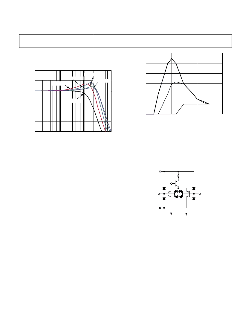
Figure 45 shows the amplifier frequency response as a G = 1
inverter with the input and output stage biased near the
negative supply rail.
Rev. C | Page 15 of 20
6
–12
0.1
100
0
FREQUENCY (MHz)
G
1
10
3
0
–3
–6
–9
V
= 5V
G = –1
V
IN
= 20mV p-p
V
S–
= –50mV
V
S–
= –100mV
V
S–
= –200mV
V
S–
= –20mV
V
S–
= –150mV
Figure 45. Small Signal Frequency Response vs. Negative Supply Bias
The input voltage (V
IN
) and reference voltage (V
IP
) are both at
0 V, (see Figure 39). +V
S
is biased at +5 V, and V
S
is swept
from 200 mV to 20 mV. With the input and output voltages
biased 200 mV above the bottom rail, the G = 1 inverter
frequency response is not much different from what is seen
with the input and output voltages biased near midsupply.
At 150 mV bias, the frequency response starts to decrease
and at 20 mV, the inverter bandwidth is less than half its
nominal value.
CAPACITANCE DRIVE
Capacitance at the output of an amplifier creates a delay within
the feedback path that, if within the bandwidth of the loop, can
create excessive ringing and oscillation. The G = +1 follower
topology has the highest loop bandwidth of any typical
configuration and, therefore, is the most vulnerable to the
effects of capacitance load.
A small resistor in series with the amplifier output and the
capacitive load mitigates the problem. Figure 46 plots the
recommended series resistance vs. capacitance for gains
of +1, +2, and +5.
60
0
10
10000
0
CAPACITANCE LOAD (pF)
S
Ω
)
50
40
30
20
10
100
1000
G = +1
G = +2
G = +5
Figure 46. Series Resistance vs. Capacitance Load
INPUT PROTECTION
The ADA4841-1/ADA4841-2 are fully protected from ESD
events, withstanding human body model ESD events of 2.5 keV
and charge device model events of 1 keV with no measured
performance degradation. The precision input is protected
with an ESD network between the power supplies and diode
clamps across the input device pair, as shown in Figure 47.
0
VP
ESD
ESD
VEE
VCC
BIAS
TO REST OF AMPLIFIER
VN
ESD
ESD
Figure 47. Input Stage and Protection Diodes
For differential voltages above approximately 1.4 V, the diode
clamps start to conduct. Too much current can cause damage
due to excessive heating. If large differential voltages need to be
sustained across the input terminals, it is recommended that the
current through the input clamps be limited to below 150 mA.
Series input resistors sized appropriately for the expected
differential overvoltage provide the needed protection.
The ESD clamps start to conduct for input voltages more than
0.7 V above the positive supply and input voltages more than
0.7 V below the negative supply. It is recommended that the
fault current be limited to less than 150 mA if an overvoltage
condition is expected.
相關PDF資料 |
PDF描述 |
|---|---|
| ADA4841-1YRZ-RL | Low Power, Low Noise and Distortion, Rail-to-Rail Output Amplifier |
| ADA4841-2YRMZ | Low Power, Low Noise and Distortion, Rail-to-Rail Output Amplifier |
| ADA4841-2YRMZ-R7 | Low Power, Low Noise and Distortion, Rail-to-Rail Output Amplifier |
| ADA4841-2YRMZ-RL | Low Power, Low Noise and Distortion, Rail-to-Rail Output Amplifier |
| ADA4841-2YRZ | Low Power, Low Noise and Distortion, Rail-to-Rail Output Amplifier |
相關代理商/技術參數 |
參數描述 |
|---|---|
| ADA4841-1YRZ-R7 | 制造商:Analog Devices 功能描述:IC OP-AMP 80MHZ 13V/S SOIC-8 |
| ADA4841-1YRZ-RL | 功能描述:IC OPAMP VF R-R LP LN 60MA 8SOIC RoHS:是 類別:集成電路 (IC) >> Linear - Amplifiers - Instrumentation 系列:- 標準包裝:50 系列:- 放大器類型:通用 電路數:2 輸出類型:滿擺幅 轉換速率:1.8 V/µs 增益帶寬積:6.5MHz -3db帶寬:4.5MHz 電流 - 輸入偏壓:5nA 電壓 - 輸入偏移:100µV 電流 - 電源:65µA 電流 - 輸出 / 通道:35mA 電壓 - 電源,單路/雙路(±):1.8 V ~ 5.25 V,±0.9 V ~ 2.625 V 工作溫度:-40°C ~ 85°C 安裝類型:表面貼裝 封裝/外殼:10-TFSOP,10-MSOP(0.118",3.00mm 寬) 供應商設備封裝:10-MSOP 包裝:管件 |
| ADA4841-2 | 制造商:AD 制造商全稱:Analog Devices 功能描述:Low Power, Low Noise and Distortion ail-to-Rail Output Amplifiers |
| ADA4841-2YCPZ-R2 | 功能描述:IC OPAMP VF R-R LP 60MA 8LFCSP RoHS:是 類別:集成電路 (IC) >> Linear - Amplifiers - Instrumentation 系列:- 標準包裝:1,000 系列:- 放大器類型:電壓反饋 電路數:4 輸出類型:滿擺幅 轉換速率:33 V/µs 增益帶寬積:20MHz -3db帶寬:30MHz 電流 - 輸入偏壓:2nA 電壓 - 輸入偏移:3000µV 電流 - 電源:2.5mA 電流 - 輸出 / 通道:30mA 電壓 - 電源,單路/雙路(±):4.5 V ~ 16.5 V,±2.25 V ~ 8.25 V 工作溫度:-40°C ~ 85°C 安裝類型:表面貼裝 封裝/外殼:14-SOIC(0.154",3.90mm 寬) 供應商設備封裝:14-SOIC 包裝:帶卷 (TR) |
| ADA4841-2YCPZ-R7 | 功能描述:運算放大器 - 運放 Dual Low Power Low Noise Rail-Rail OpAmp RoHS:否 制造商:Texas Instruments 通道數量:1 共模抑制比(最小值):120 dB 輸入補償電壓:6 V 輸入偏流(最大值):1400 pA 工作電源電壓:4 V to 36 V 安裝風格:SMD/SMT 封裝 / 箱體:SOT-23-5 轉換速度:0.8 V / us 關閉:No 輸出電流: 最大工作溫度:+ 125 C 封裝:Reel |
發布緊急采購,3分鐘左右您將得到回復。