- 您現在的位置:買賣IC網 > PDF目錄373974 > ADA4851-4 (Analog Devices, Inc.) Low Cost, High Speed, Rail-to-Rail, Output Op Amps PDF資料下載
參數資料
| 型號: | ADA4851-4 |
| 廠商: | Analog Devices, Inc. |
| 英文描述: | Low Cost, High Speed, Rail-to-Rail, Output Op Amps |
| 中文描述: | 低成本,高速,軌到軌輸出運算放大器 |
| 文件頁數: | 14/20頁 |
| 文件大小: | 325K |
| 代理商: | ADA4851-4 |
ADA4851-1/ADA4851-2/ADA4851-4
Figure 42 illustrates how the rising edge settling time for the
amplifier is configured as a unity-gain follower, stretching out
as the top of a 1 V step input that approaches and exceeds the
specified input common-mode voltage limit.
Rev. D | Page 14 of 20
For signals approaching the minus supply and inverting gain
and high positive gain configurations, the headroom limit is the
output stage. The ADA4851-1/ADA4851-2/ADA4851-4 amplifiers
use a common emitter output stage. This output stage maximizes
the available output range, limited by the saturation voltage of
the output transistors. The saturation voltage increases with the
drive current that the output transistor is required to supply due
to the output transistor’s collector resistance.
1.8
2.0
2.2
2.4
2.6
2.8
3.0
3.2
3.4
0
10
20
30
40
50
60
70
80
90
100
O
TIME (ns)
0
3.6
V
STEP
= 2V TO 3V
V
STEP
= 2.1V TO 3.1V
V
STEP
= 2.2V TO 3.2V
V
STEP
= 2.3V TO 3.3V
V
STEP
= 2.4V TO 3.4V
G = +1
R
L
= 1k
Ω
V
S
= 5V
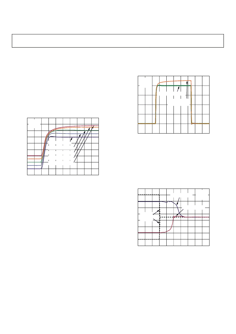
Figure 42. Output Rising Edge for 1 V Step at Input Headroom Limits
As the saturation point of the output stage is approached, the
output signal shows increasing amounts of compression and
clipping. As in the input headroom case, higher frequency
signals require a bit more headroom than the lower frequency
signals. Figure 16 illustrates this point by plotting the typical
distortion vs. the output amplitude.
OVERLOAD BEHAVIOR AND RECOVERY
Input
The specified input common-mode voltage of the ADA4851-1/
ADA4851-2/ADA4851-4 is 200 mV below the negative supply
to within 2.2 V of the positive supply. Exceeding the top limit
results in lower bandwidth and increased rise time, as seen in
Figure 41 and Figure 42. Pushing the input voltage of a unity-
gain follower to less than 2 V from the positive supply leads to
the behavior shown in Figure 43—an increasing amount of
output error as well as a much increased settling time. The
recovery time from input voltages 2.2 V or closer to the positive
supply is approximately 55 ns, which is limited by the settling
artifacts caused by transistors in the input stage coming out of
saturation.
The amplifiers do not exhibit phase reversal, even for input
voltages beyond the voltage supply rails. Going more than 0.6 V
beyond the power supplies turns on protection diodes at the input
stage, which greatly increases the current draw of the devices.
O
TIME (ns)
0
2.00
2.25
2.50
3.00
3.25
3.50
2.75
0
100
200
300
400
500
600
700
800
900
1k
G = +1
R
L
= 1k
Ω
V
S
= 5V
V
STEP
= 2.25V TO 3.25V
V
= 2.25V TO
3.5V, 4V, AND 5V
Figure 43. Pulse Response of G = 1 Follower,
Input Step Overloading the Input Stage
Output
Output overload recovery is typically within 35 ns after the
amplifier’s input is brought to a nonoverloading value. Figure 44
shows output recovery transients for the amplifier configured in
an inverting gain of 1 recovering from a saturated output from
the top and bottom supplies to a point at midsupply.
–2
–1
0
1
2
3
4
5
6
0
10
20
30
40
50
60
70
80
90
100
I
TIME (ns)
0
7
G = –1
R
L
= 1k
Ω
V
S
= 5V
INPUT
VOLTAGE
EDGES
V
OUT
= 5V TO 2.5V
V
OUT
= 0V TO 2.5V
Figure 44. Overload Recovery
相關PDF資料 |
PDF描述 |
|---|---|
| ADA4851-2 | Low Cost, High Speed, Rail-to-Rail, Output Op Amps |
| ADA4899-1 | Unity Gain Stable, Ultralow Distortion, 1 nV/ Hz Voltage Noise, High Speed Op Amp |
| ADA4899-1YCPZ-R2 | Unity Gain Stable, Ultralow Distortion, 1 nV/ Hz Voltage Noise, High Speed Op Amp |
| ADA4899-1YCPZ-R7 | Unity Gain Stable, Ultralow Distortion, 1 nV/ Hz Voltage Noise, High Speed Op Amp |
| ADA4899-1YCPZ-RL | Unity Gain Stable, Ultralow Distortion, 1 nV/ Hz Voltage Noise, High Speed Op Amp |
相關代理商/技術參數 |
參數描述 |
|---|---|
| ADA4851-4WYRUZ-R7 | 功能描述:IC OPAMP QUAD R-R HS 14-TSSOP RoHS:是 類別:集成電路 (IC) >> Linear - Amplifiers - Instrumentation 系列:- 標準包裝:2,500 系列:- 放大器類型:通用 電路數:1 輸出類型:滿擺幅 轉換速率:0.11 V/µs 增益帶寬積:350kHz -3db帶寬:- 電流 - 輸入偏壓:4nA 電壓 - 輸入偏移:20µV 電流 - 電源:260µA 電流 - 輸出 / 通道:20mA 電壓 - 電源,單路/雙路(±):2.7 V ~ 36 V,±1.35 V ~ 18 V 工作溫度:-40°C ~ 85°C 安裝類型:表面貼裝 封裝/外殼:8-SOIC(0.154",3.90mm 寬) 供應商設備封裝:8-SO 包裝:帶卷 (TR) |
| ADA4851-4YRU-EBZ | 功能描述:BOARD EVAL FOR ADA4851-4YRU RoHS:是 類別:編程器,開發系統 >> 評估板 - 運算放大器 系列:- 產品培訓模塊:Lead (SnPb) Finish for COTS Obsolescence Mitigation Program 標準包裝:1 系列:- |
| ADA4851-4YRUZ | 功能描述:IC OPAMP VF R-R QUAD LP 14TSSOP RoHS:是 類別:集成電路 (IC) >> Linear - Amplifiers - Instrumentation 系列:- 標準包裝:100 系列:- 放大器類型:通用 電路數:1 輸出類型:- 轉換速率:0.2 V/µs 增益帶寬積:- -3db帶寬:- 電流 - 輸入偏壓:100pA 電壓 - 輸入偏移:30µV 電流 - 電源:380µA 電流 - 輸出 / 通道:- 電壓 - 電源,單路/雙路(±):±2 V ~ 18 V 工作溫度:0°C ~ 70°C 安裝類型:表面貼裝 封裝/外殼:8-SOIC(0.154",3.90mm 寬) 供應商設備封裝:8-SO 包裝:管件 |
| ADA4851-4YRUZ-R7 | 制造商:AD 制造商全稱:Analog Devices 功能描述:Low Cost, High Speed, Rail-to-Rail Output Op Amps |
| ADA4851-4YRUZ-RL | 功能描述:IC OPAMP VF R-R QUAD LP 14TSSOP RoHS:是 類別:集成電路 (IC) >> Linear - Amplifiers - Instrumentation 系列:- 標準包裝:2,500 系列:- 放大器類型:通用 電路數:1 輸出類型:滿擺幅 轉換速率:0.11 V/µs 增益帶寬積:350kHz -3db帶寬:- 電流 - 輸入偏壓:4nA 電壓 - 輸入偏移:20µV 電流 - 電源:260µA 電流 - 輸出 / 通道:20mA 電壓 - 電源,單路/雙路(±):2.7 V ~ 36 V,±1.35 V ~ 18 V 工作溫度:-40°C ~ 85°C 安裝類型:表面貼裝 封裝/外殼:8-SOIC(0.154",3.90mm 寬) 供應商設備封裝:8-SO 包裝:帶卷 (TR) |
發布緊急采購,3分鐘左右您將得到回復。